


Gerber Files Explained: PCB Layers, Formats & Export

As electronic computer-aided design (ECAD) software replaced manual drafting tables in the 1970s and 1980s, fabricators needed a universal vector format to drive automated photoplotters. A photoplotter manufacturer known as Gerber Scientific developed a vector graphic format that quickly became the worldwide standard for hardware manufacturing outputs.
Today, even with direct imaging laser systems, a Gerber file remains the universal bridge between digital ECAD design software and physical circuit board fabrication. Understanding how these files determine physical board layers, how they differ from native CAD project files, and how to verify a complete PCB manufacturing package prevents fabrication delays and costly board re-spins.
Key Takeaways
- Each Gerber file represents a single 2D layer or mechanical feature of a physical PCB.
- A complete PCB manufacturing package requires a Gerber files PCB package combined with separate NC drill files and fabrication notes.
- Independent inspection using a 2D Gerber viewer before releasing files to fabrication catches alignment, revision, and layer masking errors.
What Is a Gerber File?
A Gerber file is a standardized 2D vector image format used by Computer-Aided Manufacturing (CAM) systems to direct photoplotters, which generate high-precision artwork films for PCB fabrication, and direct-imaging lasers, which project circuit patterns directly onto photoresist-coated copper without requiring film. Rather than treating a circuit board as a complex 3D object, the Gerber file format breaks a PCB design down into individual 2D image slices representing specific physical layers of the board.
A complete board layout cannot exist within a single file. Instead, the export process generates a collection of PCB fabrication files, where each file defines a specific layer:
- Top copper
- Bottom copper
- Internal signal planes
- Solder mask boundaries
- Silkscreen text
- Mechanical routings
Understanding what a Gerber file represents requires understanding the difference between manufacturing outputs from design-source data. A Gerber file contains pure vector geometry: lines, flashes, polygons, and arc coordinates, without electrical functionalities. It does not contain schematic logic, component footprints, netlists, or constraint rules.
Evolution of the Gerber Format
- RS-274D (Standard Gerber): The legacy vector format required an external wheel table (aperture file) to interpret line widths and shape definitions. Because aperture tables were supplied separately, missing or mismatched aperture files frequently corrupted board geometries.
- RS-274X (Extended Gerber): The widely used standard embeds aperture definitions, units, and coordinate formatting directly into the file header, eliminating external aperture table dependency.
- Gerber X2: The modern extension adds intelligent attributes to the file structure, defining specific layer stackup order, board function (e.g., top copper vs inner plane), and component pin locations directly within the data.
- Gerber X3: This latest extension integrates assembly data directly into the PCB file set by adding dedicated component layers. It embeds reference designators, manufacturer part numbers, and pick-and-place centroid locations. This unifies fabrication and assembly into a single workflow, automating machine programming while remaining fully backward-compatible with legacy viewers.
What Files Are Included in a Gerber Package For a 2-Layer PCB?
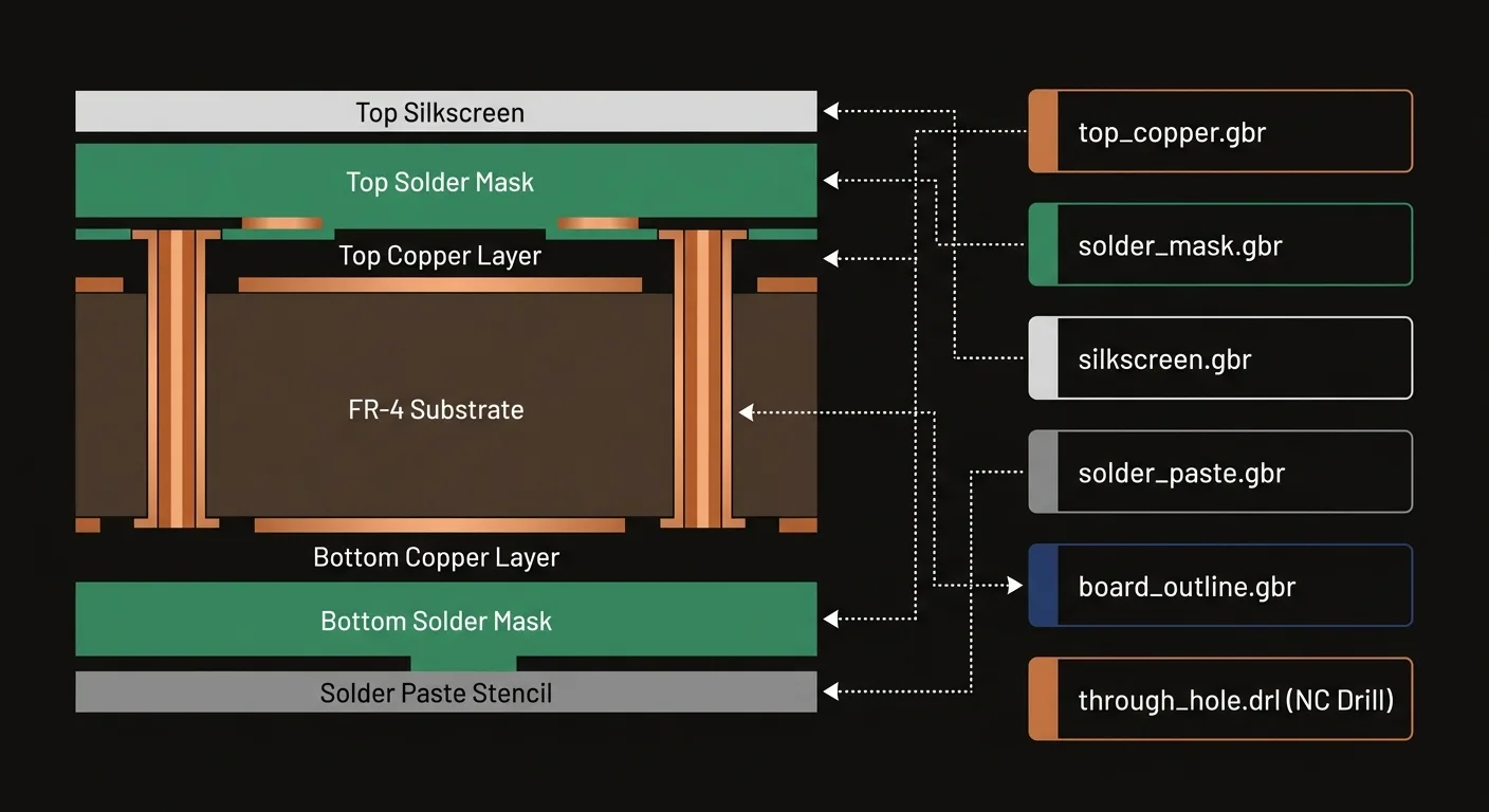
Generating a complete set of PCB manufacturing files requires exporting vector data for every physical layer alongside mechanical drilling instructions.
Summary of What Gerber Files Contain
| Layer or File Type | What It Defines | Typical Contents |
|---|---|---|
| Copper Layers | Conductive pathways and pours | Signal traces, power planes, SMT pads, thru-hole pads |
| Solder Mask | Insulation openings | Areas where protective epoxy mask is omitted to expose copper pads |
| Silkscreen | Visual labels and markings | Reference designators, pin 1 indicators, logos, warning text |
| Solder Paste | Stencil aperture boundaries | Openings for SMT paste deposition during assembly |
| Board Outline | Mechanical geometry | Outer board perimeter, internal slots, routed cutouts |
Gerber Files vs PCB Files and Drill Data
Engineering teams frequently confuse source design files (e.g. PCB files) with manufacturing outputs (e.g., gerber files). Understanding gerber files vs PCB files helps designers send correct deliverables to fabrication houses.
- A native PCB file (such as a KiCad .kicad_pcb or Altium .PcbDoc file) represents the editable CAD database. Such a file contains active components, net connectivity, clearance rules, and parametric footprints.
- Fabricators generally request flattened PCB fabrication files rather than native CAD project files because native files depend on specific software versions, proprietary fonts, and installed library paths.
- PCB Drill files are supplied separately from standard vector layer files. CNC drilling machinery utilizes NC drill formats (such as Excellon) that specify drill bit diameters, tool numbers, and exact X/Y hole coordinates.
Differences Between PCB Manufacturing File Types
| Characteristic | Gerber Files | Drill Files | Native PCB File |
|---|---|---|---|
| Primary Purpose | Manufacturing layer geometry | CNC hole drilling data | Editable layout and schematic source |
| Format Type | 2D Vector (RS-274X / Gerber X2) | NC Drill (Excellon) | Proprietary database / CAD format |
| Intelligence | Geometric shapes and traces | Tool size and X/Y coordinates | Full netlists, components, and DRC rules |
| Compatibility | Universal across all fabricators | Universal across CNC drill systems | Software-specific (requires specific ECAD tool) |
How to Generate and Review Gerber Files
Executing a PCB Gerber export requires verifying design constraints before generating output files.
Step-by-Step Export and Inspection Process
- Run DRC and ERC: Perform complete Design Rules Checking (DRC) and Electrical Rules Checking (ERC) within the ECAD tool to resolve unrouted traces or clearance violations.
- Confirm Mechanical Layers: Verify that the board outline is closed, continuous, and drawn on a dedicated mechanical layer.
- Export Gerber Vector Data: Configure export settings for RS-274X or Gerber X2. While both formats contain the required PCB layer, Gerber X2 includes embedded layer metadata and fabrication attributes that improve automation and reduce manufacturing errors. Export all required copper, solder mask, silkscreen, paste, and mechanical layers.
- Generate NC Drill Files: Export separate drill files for plated through-holes (PTH) and non-plated through-holes (NPTH), ensuring units and coordinate resolutions match the Gerber export settings.
- Compile Fabrication Notes: Include stackup specifications, copper weight requirements, surface finish preferences, and solder mask colors in a text file or fabrication drawing.
- Inspect in a Standalone Viewer: Load the exported ZIP archive into an independent 2D Gerber viewer to verify geometry prior to release.
Pre-Release Verification Checklist
- Are all required copper, solder mask, silkscreen, and mechanical layers exported?
- Do drill hole coordinates align perfectly with copper pad centers?
- Is the board outline continuous, closed, and located on a dedicated mechanical layer?
- Are solder mask openings correctly defined for all SMT pads and test points?
- Is silkscreen text legible and kept clear of exposed copper pads?
- Are internal slots, cutouts, and routing paths clearly documented?
- Have obsolete or older export files been purged from the ZIP release archive?
Common Gerber Export Mistakes
Fabrication delays frequently occur due to file packaging errors. Avoiding common pitfalls ensures a smooth transition from CAD design to physical board delivery:
- Revision Mismatches: Including copper layers from Revision B alongside a drill file exported from Revision A causes misaligned holes and broken net connections.
- Missing Board Outline: Omitting the mechanical edge layer forces the fabricator to guess board dimensions or pause production to issue an engineering query.
- Unmatched Coordinate Units: Exporting Gerber layers in metric units while exporting drill files in imperial units results in severe scaling and alignment errors in the fabricator's CAM software.
- Inverted or Mirrored Layers: Accidentally mirroring bottom copper or top silkscreen layers during export results in unworkable PCBs.
- Silkscreen Over Solder Pads: Allowing silkscreen ink to overlap exposed copper pads causes soldering defects during SMT assembly.
- Leftover Legacy Files: Archiving multiple export attempts in the same release folder confuses CAM operators regarding which files represent the final revision.
How Modern PCB Tools Simplify Manufacturing Outputs
Disconnected design software creates friction during manufacturing handoffs, where schematic updates, board layouts, and exported files exist as separate desktop artifacts.
Modern cloud-native platforms like Flux streamline manufacturing handoffs by maintaining connected schematic, layout, and output data in a single workspace. Built-in design rule checks and centralized revision control ensure that exported files accurately reflect the active design state. By providing a shared source of truth, engineering teams and fabricators can conduct collaborative design reviews directly in the browser, reducing revision errors before releasing a PCB manufacturing package. Try Flux now to simplify PCB manufacturing handoffs and ensure production files are always up to date.
FAQs
A Gerber file is a 2D vector graphic file describing an individual physical layer of a printed circuit board for manufacturing.
Fabrication requires a complete PCB manufacturing package containing gerber files for all copper, solder mask, silkscreen, and mechanical layers, combined with NC drill files and fabrication specifications.
No. Drill data is generated separately as NC drill files (typically in Excellon format) specifying exact hole coordinates and tool diameters.
A PCB file is an editable CAD design database containing netlists, active components, and layout rules. A Gerber file is a flattened 2D vector manufacturing file containing pure layer geometry without circuit intelligence.
Opening and inspecting gerber files requires utilizing a standalone 2D Gerber viewer software or web tool.
Designers load the complete ZIP archive into an independent Gerber viewer to check layer alignment, verify solder mask clearances, inspect silkscreen legibility, and confirm drill hole registration.
Yes. While formats like ODB++ and IPC-2581 exist, the Gerber file format (specifically Extended RS-274X and Gerber X2) remains the global standard for PCB fabrication.
More in Business & Strategy Library

Is Your Hardware Startup Idea Worth Building?

Collaborative PCB Design: Why Hardware Teams Are Moving to the Cloud

Electronic Component Sourcing: Lead Times & Component Lifecycles

Design for Manufacturing: How to Move from Prototype to Production

PCB Cost Optimization: How to Reduce Manufacturing Costs

Designing PCBs for IoT Devices: Key Considerations

5 Common Mistakes Working with PCB Contractors

The Hardware Founder’s Bookshelf

Design with Real-Time Supply Chain Visibility

PCB Trade Secrets vs. Patents: How Hardware Founders Protect Electronics IP

Hardware Patent Strategy for PCB Engineers: 8 Pitfalls to Avoid

What is a Defensive Publication? (vs. Patents and Trade Secrets)

Git for Hardware: Version Control for PCB Design Teams

PCB Version Control Explained: How Hardware Teams Track Design Changes

PCB Design History and Revision Management Best Practices

Real-Time PCB Collaboration: How Modern Teams Design Together

AI Gives You the Power of an Entire Supply-Chain Team

PCB Component Libraries: Best Practices for Managing Parts

How to Create and Manage PCB Footprint Libraries

PCB Library Management: How to Standardize Components Across Teams

Flux for Librarians

Prototyping vs. Production-Ready Electrical Engineering

PCB Manufacturing Process Explained Step-by-Step

PCB Design Documentation: What Every Manufacturing Package Should Include

PCB Design for Manufacturability (DFM): Rules and Best Practices

Panelization in PCB Manufacturing: Methods and Best Practices

PCB Prototyping vs. Fabrication: Which Process Is Right for Your Project?

PCB Reverse Engineering: How It Works and When to Use It

PCB Testing Methods: Ensuring Quality and Reliability

Discovering PCB Manufacturing: Technologies That Shape the Industry

What Is PCBA? PCB vs PCBA and Assembly Explained

What Is a Reflow Oven? PCB Reflow Soldering Explained

Troubleshooting JLCPCB Gerber Upload and CAM Tool Compatibility Errors
Let’s start building.

Let’s build your idea together. All you need to do is describe what you want to make, or what problem you want to solve. Flux will work with you to make it a reality.
