June 2, 2026
Designing PCBs for IoT Devices: Key Considerations
Share

An IoT PCB design is not simply a smaller version of a traditional board, it's a different class of engineering problem. Where a conventional board prioritizes point-to-point electrical connections with relatively forgiving spatial margins, an IoT design forces you to integrate delicate analog sensors, noisy digital processing, power management, and RF transceivers into a severely constrained physical footprint, all while running on, for example, a coin cell battery, for years.
To achieve such a high density, you have to move beyond standard through-hole and basic surface-mount rules. Instead, you must rely on high-density interconnects (HDI's). HDI PCBs use sequential lamination and microvia technology to pack more components and interconnections into a smaller footprint, eliminating the need for excessive layer counts while improving signal integrity. To understand how HDI boards manage this density, look closely at the interconnects themselves. Per IPC-2226, microvias are laser-drilled interconnects with a finished diameter of 150 µm or less. By using blind and buried microvias, you free up internal routing layers to manage the complex mixed-signal domains that IoT designs demand.
Power optimization dictates every component selection decision in a battery-powered design. You cannot simply drop in standard voltage regulators and expect a coin cell to last two years. Every microamp of leakage current compounds over time, and the components you choose set the floor.
For DC-DC conversion, parts like the Texas Instruments TPS62840 show what's possible at the low end. The TPS62840 is a high-efficiency step-down converter with an ultra-low operating quiescent current of typically 60 nA. The device contains special circuitry to achieve just 120 nA Iq in 100% mode to further extend battery life near the end of discharge. Pairing a power management IC (PMIC) like this with intelligent system sleep states is how to achieve your desired real-world battery life.
The sleep strategy of the microcontroller matters just as much as the PMIC. Take the Nordic nRF52840, for instance, a Bluetooth chip that is highly popular for IoT PCB design. Power consumption in a System OFF mode on the nRF52840 averages between 1.4 and 5.2 microamps, depending on the wake-up source — compared to 6.40 mA during active BLE transmission at 0 dBm. That three-order-of-magnitude swing is why duty cycle management is the single biggest lever you have on battery life.
Beyond component selection, apply these layout-level strategies:
RF layout errors don't just hurt range, they also drain the battery. A flawed matching network reduces antenna efficiency, which forces the radio to retransmit dropped packets and burn current doing it. Getting the RF right the first time is a power problem as much as a signal problem.
When you integrate protocols like BLE, Wi-Fi, LoRa, or Zigbee, you should be mindful of your layout. Where you place RF parts directly dictates your wireless range and current draw. To keep trace impedance steady, you must route your 50-ohm RF lines over a solid, flat reference plane. If you break that ground plane, you invite trouble. Even a minor shift in trace width or board thickness causes signal bounce. This signal bounce directly degrades your link budget.
| Protocol | Frequency | Typical Range | Power Draw | Best Use Case |
|---|---|---|---|---|
| BLE | 2.4 GHz | Up to 100 m | Very Low | Wearables, smart home sensors |
| Wi-Fi | 2.4 / 5 GHz | Up to 150 m | High | High-bandwidth data streaming |
| LoRa | Sub-GHz (868/915 MHz) | Up to 15 km | Very Low | Remote agriculture, smart meters |
| Zigbee | 2.4 GHz | Up to 100 m | Low | Mesh network device integration |
Note: Range figures are line-of-sight estimates. Indoor performance varies significantly based on antenna design, environment, and transmit power. The LoRa 15 km figure represents a best-case, open-field specification.
Plan your return paths before you route a single signal. A poorly planned return path creates a loop antenna that radiates noise across the entire board, noise that will affect your analog sensor inputs.
For a standard BLE or Wi-Fi IoT device, a 4- to 6-layer stack-up is typically required. Dedicated internal layers for ground and power provide the shielding sensitive signals need. Furthermore, layer transitions should be accompanied by ground stitching vias to keep the return path continuous for high-frequency signals.
Follow the following layout rules for dependable performance:
These errors often show up on first prototypes and, more expensively, in field failures.
Violating antenna keep-out zones is the most common RF mistake. Placing copper pours, vias, or even a battery casing directly under a chip antenna detunes the resonant frequency and collapses wireless range. The keep-out zone in the antenna datasheet is not a suggestion but a hard constraint validated by the manufacturer's own characterization data.
Ignoring thermal management in compact enclosures is a second major mistake. Even low-power MCUs and PMICs generate heat, and in a sealed plastic enclosure that heat has nowhere to go. To prevent hardware failure, you must build thermal escape routes directly into the board. Thermal vias and copper pours conduct heat away from active components before it becomes a reliability problem.
Undersizing power traces for peak TX current is a third major mistake. Radios draw power in short bursts, so looking only at average drain is highly misleading. For example, returning to the nRF52840 chip, a single BLE burst pulls over 6 mA. If you size a trace for the much lower average current, you create a resistive voltage drop during these spikes. This sudden voltage dip can trigger sudden chip resets, so always size your trace width for the worst-case peak, not the average.
Traditional software silos isolate mechanical, electrical, and firmware teams, which turns every enclosure interference issue or pinout mismatch into a multi-day correction cycle. For IoT hardware where size, power, and RF constraints are all interdependent, that kind of friction kills iteration speed.
Platforms like Flux are built specifically for this. Real-time collaboration lets your entire team work on schematics and layout simultaneously rather than passing files back and forth. Instead of deriving RF impedance matching networks from scratch on each new design, you can pull in verified, reusable hardware blocks for wireless modules and power management circuits. For startup teams racing to validate hardware under schedule pressure, that reuse is the difference between hitting a prototype deadline and missing it.
Try Flux and experience a faster, more reliable way to move from idea to manufacturable hardware.
Balancing dense component placements with unforgiving power and RF constraints is the reality of modern hardware engineering. When you are ready to tackle your next IoT PCB design, bringing your team into a unified environment is the most effective next step. Flux offers real-time collaboration, verified reusable RF blocks, and an integrated EDA platform that helps you iterate faster and catch costly errors before fabrication.


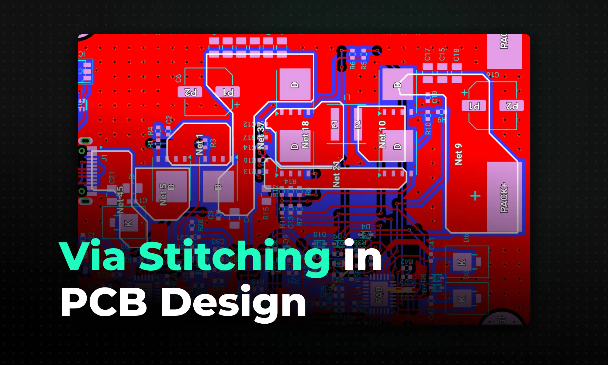
A practical guide to via stitching in PCB design -- what it is, why it improves EMI, signal integrity, and thermal performance, and where to place stitching vias. Includes spacing rules (like lambda/20), design guidelines, common mistakes to avoid, and how Flux can automate stitching via placement.

A guide to PCB component selection, covering electrical specs, footprints, thermal performance, sourcing, and best practices for picking parts that ship reliably.

A guide to PCB design reviews, covering schematic, layout, and DFM checks engineers use to catch errors early and ship more reliable boards.

A guide to creating and managing PCB footprint libraries, covering IPC standards, pad sizing, validation workflows, and best practices for reliable land patterns.

A guide to PCB schematic best practices, covering organization, symbols, labeling, and readability tips for clean, maintainable circuit diagrams.

A guide to flexible PCB design, covering materials, stackups, bend radius, and layout best practices for wearables, medical devices, and other compact electronics.

A beginner-friendly guide to reading PCB schematics, covering common symbols, nets, and how to follow signal flow through a circuit diagram.

An overview of collaborative PCB design, showing how cloud-native tools, real-time editing, and shared libraries are reshaping modern hardware team workflows.
