June 5, 2026
Collaborative PCB Design: Why Hardware Teams Are Moving to the Cloud
Share

Legacy desktop EDA software physically isolates design data on individual machines, and that single architectural choice creates a cascade of problems for any team larger than one. The standard handoff procedure of zipping the project folder, emailing, and waiting for feedback produces unversioned duplicate copies of the same board. Two engineers can't touch the same file simultaneously without one overwriting the other's work on merge.
These siloed workflows produce predictable, recurring failure modes:
The deeper problem is that none of this scales. A two-person team can manage it with discipline. A five-person team across two time zones cannot.
Collaborative PCB design replaces localized project files with a centralized, cloud-hosted environment where multiple engineers interact with the same design data simultaneously. Rather than a solitary desktop application, the platform becomes a shared workspace that synchronizes schematic capture, layout routing, and component libraries across the entire team in real time.
The core requirement is continuous visibility: every team member sees the same design state at any given moment, with no manual syncing required. To support this, collaborative hardware platforms are built on three structural pillars:
Migrating to cloud PCB design eliminates redundant data duplication and shortens the entire hardware review cycle. The most immediate gain is centralized version control: cloud workspaces track revisions automatically, letting you roll back to a known-good state without hunting through a folder of files named "schematic_final_v3_REAL.sch."
Beyond versioning, cloud EDA tools change how component libraries work. Instead of each engineer maintaining a local footprint database that drifts out of sync, the team draws from a single source hosted online. Design reviews shift from static PDF markups into interactive sessions where reviewers can measure clearances and leave comments directly on the live layout.
| Feature | Traditional Desktop EDA | Cloud PCB Design Tools |
|---|---|---|
| Data Storage | Local drives and fragmented network folders | Centralized cloud workspaces |
| Concurrent Editing | Sequential only; requires manual file locking | Real-time simultaneous multi-user editing |
| Library Management | Local libraries prone to divergence | Single-source-of-truth cloud component library |
| Design Reviews | Exported PDFs and manual redlining | Interactive browser-based viewing and markup |
| Version History | Manual file naming conventions | Automated revision tracking with rollback |
Bringing a hardware product to market now requires coordinating globally distributed specialists across electrical, mechanical, and supply chain domains. Fast-moving hardware startups and enterprise teams both depend on cross-functional collaboration to finalize complex electromechanical assemblies, and the old localized-file model breaks down fast under that pressure.
Distributed teams can't absorb the IT overhead of managing per-seat software licenses and VPN infrastructure across time zones. They need frictionless access to live design data to hit aggressive release schedules. Cloud hardware tools address these dynamics directly:
Transitioning a hardware team to cloud EDA is not without friction, and the concerns engineering managers raise are legitimate. Hosting proprietary schematics on external servers is a real risk calculation, particularly in regulated sectors like defense and medical devices.
Reputable platforms address this directly. Altium 365 GovCloud, for example, is a dedicated region operated exclusively by US persons within AWS GovCloud, built to meet the compliance demands of the Defense Industrial Base. Data is hosted through AWS and encrypted using XTS-AES-256 at rest and TLS 1.2 in transit. Access is managed through granular role-based permissions, so viewers, designers, and administrators only see what they are authorized to see.
Even with strong security infrastructure in place, teams must manage the transition actively:
Flux was built to solve collaboration bottlenecks by moving the entire hardware design process into a browser-native, multiplayer environment. There is no client to install: engineers on Windows, Mac, or Linux open a project instantly via URL, which eliminates OS compatibility issues and removes the IT overhead of managing software installations across a distributed team.
Flux is, from the start, a team-based collaborative system where collaboration is integral to the design process. Multiple team members can work on the design simultaneously, with each able to use the AI assistant for design guidance, documentation, and reference. Think of it as Google Docs for PCB layout: sharing with contractors, collaborators, and clients is as easy as sharing a link. You invite others to collaborate, control permissions, and drop comments directly on the design, with automated version control tracking every change.
The platform's key collaboration features include:
Flux Copilot, the platform's integrated AI co-designer, extends this further. Copilot can take on the role of co-designer, interpreting a designer's idea, wiring up the schematic, and producing the PCB layout and bill of materials. Flux Copilot also makes component suggestions, such as bypass capacitors or pull-up/pull-down resistors, based on specifications pulled from IC datasheets, and at each step asks the designer to make the final decision, allowing substitutions or modifications along the way. Copilot also performs AI design reviews, checking for overlooked details like missing decoupling capacitors, saving you from costly errors. The engineer stays in the director's seat; Copilot handles the tedious execution.
Ready to untangle your hardware workflow and move beyond outdated file sharing? Modern teams require continuous visibility, real-time sync, and the elimination of manual library management. Start your collaborative PCB design journey today by building your next project in Flux for free.


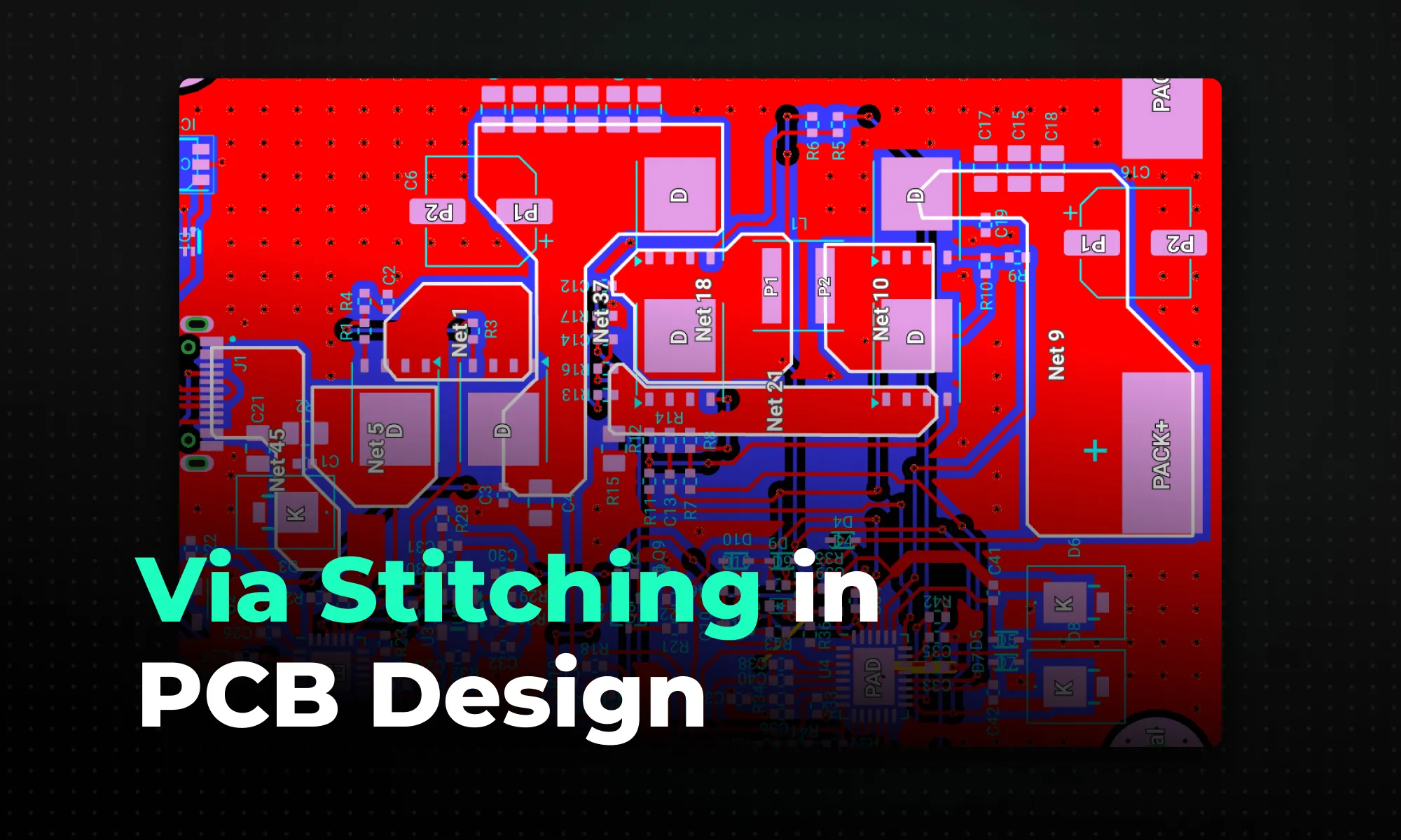
A practical guide to via stitching in PCB design -- what it is, why it improves EMI, signal integrity, and thermal performance, and where to place stitching vias. Includes spacing rules (like lambda/20), design guidelines, common mistakes to avoid, and how Flux can automate stitching via placement.
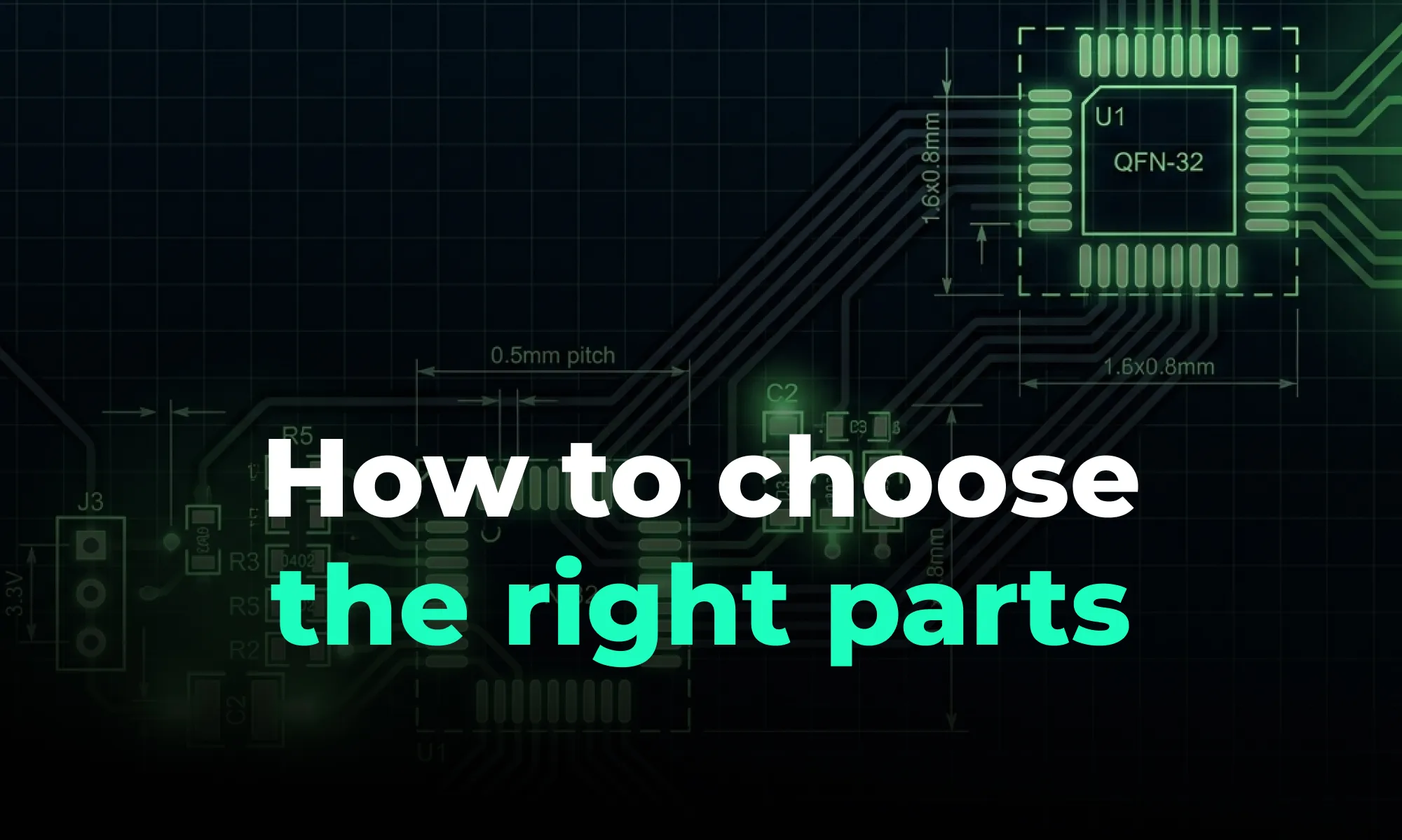
A guide to PCB component selection, covering electrical specs, footprints, thermal performance, sourcing, and best practices for picking parts that ship reliably.

A guide to PCB design reviews, covering schematic, layout, and DFM checks engineers use to catch errors early and ship more reliable boards.

A guide to creating and managing PCB footprint libraries, covering IPC standards, pad sizing, validation workflows, and best practices for reliable land patterns.

A guide to PCB schematic best practices, covering organization, symbols, labeling, and readability tips for clean, maintainable circuit diagrams.

A guide to flexible PCB design, covering materials, stackups, bend radius, and layout best practices for wearables, medical devices, and other compact electronics.

A beginner-friendly guide to reading PCB schematics, covering common symbols, nets, and how to follow signal flow through a circuit diagram.

A guide to managing PCB component libraries, covering symbols, footprints, and 3D models with best practices for standardizing parts across hardware teams.
