March 16, 2026
What is Schematic Design? All You Need to Know
Share

From symbols and signal flow to schematic capture and PCB handoff — a complete guide for engineers and beginners alike.
If you're new to electronics, schematic design is probably one of the first things you'll run into and also one of the first things that makes you go "wait, what am I looking at?"
Simply put, schematic design is the process of mapping out an electronic circuit using symbols and lines before anything gets built. Think of it as the planning stage. Before a single component touches a board, engineers use a schematic to figure out every electrical connection, how components relate to each other, and where signals flow.
It's not about how the circuit looks physically. It's about how it works electrically. That distinction matters a lot, especially when you're just starting out.
A good schematic does three things: it shows how components connect through wires and nets, how parts depend on each other functionally, and which direction data, power, and control signals travel.
Catching mistakes at this stage is also way cheaper than catching them after a board has already been manufactured. And beyond that, a schematic becomes the shared language for everyone working on a project; engineers, firmware developers, and the manufacturing team all refer back to it.
A schematic diagram is the actual drawing, it's the visual output of the schematic design process. It uses standardized symbols to represent components and lines to show how they connect.
One thing that trips up a lot of beginners: a schematic diagram is not a picture of your circuit. A resistor symbol looks the same whether the physical part is tiny and surface-mounted or large and through-hole. The diagram doesn't care about size or shape, it only cares about electrical relationships.

Engineers typically read schematics left to right, top to bottom, with inputs on the left and outputs on the right. Once you get used to that flow, tracing how a circuit behaves becomes a lot more natural.
Worth keeping in mind: a schematic shows logical connectivity. A PCB layout shows physical placement and routing. Both matter, but they're answering different questions at different points in the design process.
Schematics use a visual language made up of standardized symbols, defined by standards like IEEE 315 and IEC 60617 so that any engineer anywhere can pick one up and read it.
You don't need to memorize all of them at once. Start with these six and you'll be able to follow most basic schematics:

From there, you'll gradually pick up symbols for inductors, op-amps, MOSFETs, voltage regulators, connectors, and more. But these six are the foundation.
Once you have a circuit design in mind, you need to get it into a computer in a format that design tools can actually use. That process is called schematic capture.
You're essentially taking your idea — whether it's a sketch on paper or just a concept in your head — and turning it into a structured digital schematic using EDA (Electronic Design Automation) software. You place component symbols, draw connections between them, assign reference designators like R1, C1, U1, and fill in component values.
The result isn't just a drawing. It's machine-readable data that your toolchain can process downstream.
When you're done, the tool generates two things you'll use constantly:
Popular EDA tools for schematic capture include KiCad, Altium Designer, Cadence OrCAD, and newer browser-based platforms like Flux. Most modern tools also include real-time electrical rules checking (ERC), which automatically flags problems like unconnected pins, missing power references, or conflicting net names before a designer moves to layout.
The general flow goes: Schematic capture → ERC validation → netlist export → PCB layout → design rule check (DRC) → Gerber file generation → manufacturing. Get something wrong early and it ripples through everything downstream.
Ready to start your first schematic? Follow Flux step-by-step guide to designing your first project. Start your first schematic in Flux.
People often use "schematic" and "PCB layout" interchangeably, but they're really two separate things — and confusing them is a common beginner mistake.
The short version: a schematic is logical, a PCB layout is physical.
A good way to think about it: if the schematic is the wiring diagram of a building's electrical system, the PCB layout is the construction blueprint — showing exactly where cables run through the walls, how far apart conduits need to be, and which breakers connect where.
Neither replaces the other. A clean schematic doesn't guarantee your board will be manufacturable, and a beautifully routed PCB means nothing if the underlying schematic has a wiring error.
That said, the gap between schematic and finished layout is narrowing fast. Flux AI Auto-Layout feature lets engineers go from a verified schematic to a routed PCB with a single click, automatically placing components (already in beta), routing traces, prioritizing critical power paths, and delivering results clean enough to manufacture with minimal cleanup. Powered by reinforcement learning, it's a fundamentally different approach to PCB layout, and a glimpse at where the entire discipline is heading.
Even engineers who've been doing this for years make schematic mistakes. The tricky part is that some of them don't show up until the board comes back from fabrication, which is an expensive way to find out something went wrong.
Here are the ones worth watching out for:
With most traditional EDA tools like KiCad, Altium Designer, Cadence OrCAD, running an ERC is a manual step, it's something you remember to do when you think you're done, and hope you didn't miss anything in between.
In Flux handles this differently: ERC runs automatically in the background as you design, so issues get flagged in real time before they have a chance to pile up.
For a long time, schematic design meant installing heavyweight desktop software, managing licenses, and working in isolation. Tools like Altium Designer and Cadence Allegro are good, but they were built for a world where hardware teams sat in the same office.
That world has changed. Teams are distributed, timelines are shorter, and the expectation is that design tools should work the way modern software does, in the browser, collaboratively, without friction.
Hardware design is moving in the same direction software development did a decade ago, toward tools that are faster, more collaborative, and less painful to use. The days of emailing locked design files are numbered.


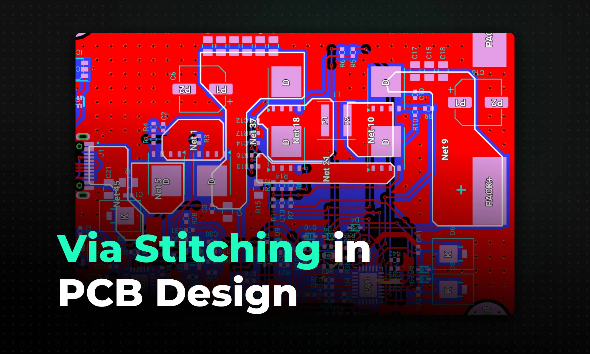
A practical guide to via stitching in PCB design -- what it is, why it improves EMI, signal integrity, and thermal performance, and where to place stitching vias. Includes spacing rules (like lambda/20), design guidelines, common mistakes to avoid, and how Flux can automate stitching via placement.
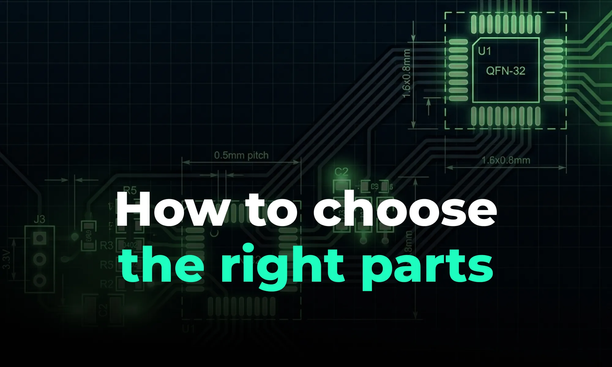
A guide to PCB component selection, covering electrical specs, footprints, thermal performance, sourcing, and best practices for picking parts that ship reliably.

A guide to PCB design reviews, covering schematic, layout, and DFM checks engineers use to catch errors early and ship more reliable boards.

A guide to creating and managing PCB footprint libraries, covering IPC standards, pad sizing, validation workflows, and best practices for reliable land patterns.

A guide to PCB schematic best practices, covering organization, symbols, labeling, and readability tips for clean, maintainable circuit diagrams.

A guide to flexible PCB design, covering materials, stackups, bend radius, and layout best practices for wearables, medical devices, and other compact electronics.

A beginner-friendly guide to reading PCB schematics, covering common symbols, nets, and how to follow signal flow through a circuit diagram.

An overview of collaborative PCB design, showing how cloud-native tools, real-time editing, and shared libraries are reshaping modern hardware team workflows.
