April 21, 2026
Blind Vias, Buried Vias, and Microvias: A Complete Guide to PCB Via Types
Share

The IPC-T-50 standard defines a via as a plated hole used as an interlayer connection, but not intended for inserting a component lead. That last clause matters. A via is strictly for layer-to-layer signal, power, or ground interconnection; it is not a component mounting hole. Plated through-holes (PTH) that accept component leads are a separate structure. Confusing the two leads to Design for Manufacturing (DFM) errors.
Every PCB via shares three anatomical elements:
Vias provide electrical connections between copper traces on different PCB layers, enabling board miniaturization. They also carry secondary functions. Vias can serve as thermal paths to improve heat transfer from power devices to a heatsink. They can also assist with circuit shielding when densely arranged to block electromagnetic waves. As component density has increased and package pitches have shrunk, a single via type can no longer serve every routing scenario. That pressure produced the family of specialized via types that defines modern multilayer PCB design.
Choosing the right via requires understanding how each type is manufactured and how it impacts your routing channels. Generally, we classify vias by their physical span across the board layers: through-hole, blind, and buried. Microvias, usually categorized in their own group, are technically just incredibly small blind or buried vias.
Through-hole vias are the simplest and most widely supported via type in PCB fabrication. A through-hole via extends through the entire thickness of the PCB, connecting every layer in the stack simultaneously. They are created by CNC mechanical drilling after full-stack lamination, then copper-plated through the barrel.
Key specifications for through-hole vias include:
The primary limitation of through-hole vias is routing real estate. Because the barrel spans every layer, the via consumes antipad clearance space on all layers, including layers that have no electrical connection to the via. On dense multilayer boards, this wastes inner-layer routing channels. For high-speed signals, through-hole vias also create stubs (the unused portion of the barrel below the last connected layer) which cause signal reflections at high frequencies.
A blind via connects tracks at an external layer to one or more tracks located in internal layers, without going through the entire board. This type of via is not visible from the opposite side of the PCB. The primary advantage is that layers the blind via does not reach remain fully available for routing. This is a meaningful benefit when inner-layer congestion is driving up layer count.
Blind vias are fabricated by one of three methods:
When creating blind vias, attention must be paid to the drilling depth. Holes that are too deep or too shallow can have negative impacts. If the holes are too deep, signal distortion or attenuation may occur. If they are too shallow, poor connections result.
Buried vias connect two or more inner layers of a PCB without reaching either of the outer layers. They are completely hidden inside the PCB and cannot be seen from either side of the board. On boards with 6 or more layers, buried vias can fully decongest both outer surfaces, leaving the top and bottom layers free for component placement and multilayer design and routing.
The critical manufacturing implication is that buried vias must be drilled and plated before the outer layers are laminated. Creating buried vias involves sequential lamination, where layers are built up step by step. This process is time-consuming and requires advanced equipment, increasing labor and tooling costs. There cannot be buried vias in a PCB with less than four layers because there are no inner layers to connect.
Per IPC-2226A, a microvia is defined as a blind or subsequently buried hole that is less than 0.15 mm in diameter having a pad diameter less than 0.35 mm. They are formed either through laser or mechanical drilling, wet/dry etching, photo imaging, or conductive ink-formation followed by a plating operation. A microvia has a maximum aspect ratio of 1:1, with a total length of no more than 0.25 mm. The typical working aspect ratio is about 0.8:1.
Microvias connect only adjacent layers. To span multiple layers, they are arranged in specific configurations:
Microvias enable extremely fine-pitch BGA routing. They are the enabling technology behind layer count reduction in HDI designs. For example, a board requiring 8 through-hole layers can often be redesigned as a 4-layer HDI board using microvias. This reduces material cost enough to partially offset the higher per-via cost.
Via type selection is a function of board layer count, routing density, component package type, cost budget, and manufacturer capability.
For 2 to 4 layer boards with standard SMD components, through-hole vias are sufficient and cost-optimal. There are no inner layers that need to remain clear of via barrels, and no BGA pitches that demand laser-drilled holes. For 4 to 8 layer moderate-density boards, blind vias become worthwhile when inner routing space is at a premium and through-hole vias are forcing additional layers.
BGA pitch is the most common trigger for advanced vias:
Transitioning to High Density Interconnect (HDI) with advanced via types can actually lower total system cost. Fewer layers with high-density build-up result in thinner, lighter, more economical boards compared to adding more through-hole layers to solve a routing congestion problem.
The table below summarizes the engineering trade-offs across all four primary via types. Use it as a quick reference before committing to a via strategy in layout.
| Via Type | Connects | Fab Method | Typical Min Diameter | Cost vs. Through-Hole | Key Use Case |
|---|---|---|---|---|---|
| Through-Hole | All layers | CNC mechanical drill | 0.15 mm | Baseline | General routing, power, connectors |
| Blind | Outer to inner | Laser or controlled-depth | 0.15 mm | +20 to 40% | HDI, moderate-density boards, BGA escape |
| Buried | Inner to inner | Sequential lamination | 0.15 mm | +30 to 50% | Dense multilayer inner routing |
| Microvia | Adjacent layers | Laser drill only | ≤0.15 mm | +40 to 60% | Fine-pitch BGA, HDI, high-speed signals |
Through-hole vias introduce stubs on every layer they pass through without connection. This physical leftover degrades signal integrity. On a standard 1.6 mm FR4 board, a via with a 10-mil drilled hole diameter and a 20-mil pad diameter adds approximately 0.42 pF of capacitance and 1.46 nH of inductance to the trace. While these parasitics matter very little at low frequencies, they become design-limiting above a few hundred megahertz.
Regarding reliability, IPC test committees report that stacked microvias can fail post-manufacturing at the metallurgical junction between layers during thermal cycling. Staggered configurations remain the lower-risk default.
Getting via geometry and placement right at layout time is far cheaper than discovering a DFM violation after tape-out. This is especially true on boards with sequential lamination.
Calculate your aspect ratio (board thickness divided by drill diameter) before any via goes in the design. A 1.6 mm board with a 0.2 mm drill gives an 8:1 aspect ratio, which is within standard limits. Push to 0.1 mm on the same board and you hit 16:1, which is unreliable at nearly all commercial fabs.
Via Design Best Practices Checklist:
Most via-related fabrication failures trace back to a small set of recurring design errors.
Excess vias on high-speed signal paths distort signals and cause reflections. Minimize layer transitions on clock lines, differential pairs, and high-speed data buses. Route on a single layer whenever the board density allows it.
Failing to fill and cap vias under BGAs allows solder to wick into the via during assembly, causing poor solder joints or open connections. This is one of the most common assembly failures on HDI boards. Via-in-pad without fill is not a valid cost-saving shortcut.
Stacking laser-drilled microvias on top of mechanically drilled blind vias without proper fill between them is a known failure mode. Vias that will end up buried after extra lamination steps must first be filled to prevent voids. Prefer staggered over stacked vias for better load distribution.
The via decisions covered in this article compound in complexity as layer count grows. An 8-layer HDI board with blind, buried, and stacked microvias needs tooling that actively enforces constraints during layout, not after.
Flux's cloud-native PCB design environment provides real-time design rule checking that catches via constraint violations as you route. Aspect ratio, annular ring, clearance, and via-in-pad fill flags are validated immediately. Flux's collaborative environment lets your fabricator's DFM constraints live inside your design rules from day one, eliminating the gap between what the designer specifies and what the fab can actually build, operating like a true AI routing assistant.
For multilayer routing, Flux's stackup visualization lets you see via spans, layer connections, and routing channels in context. When working through BGA breakout strategies on a 0.5 mm pitch component, visualizing which layers each via type reaches directly impacts whether your first layout is manufacturable or requires a complete re-spin.
Now that you understand the mechanics and use cases for every PCB via type, the next step is applying them flawlessly in your own complex layouts. Navigating tight BGA fanouts, aspect ratios, and sequential lamination rules doesn't have to be a headache. Flux's cloud-native platform brings real-time constraint validation and AI-assisted routing straight to your browser, helping you build highly manufacturable multilayer boards faster. Ready to streamline your routing process? Sign up for Flux today and transform how you design hardware.


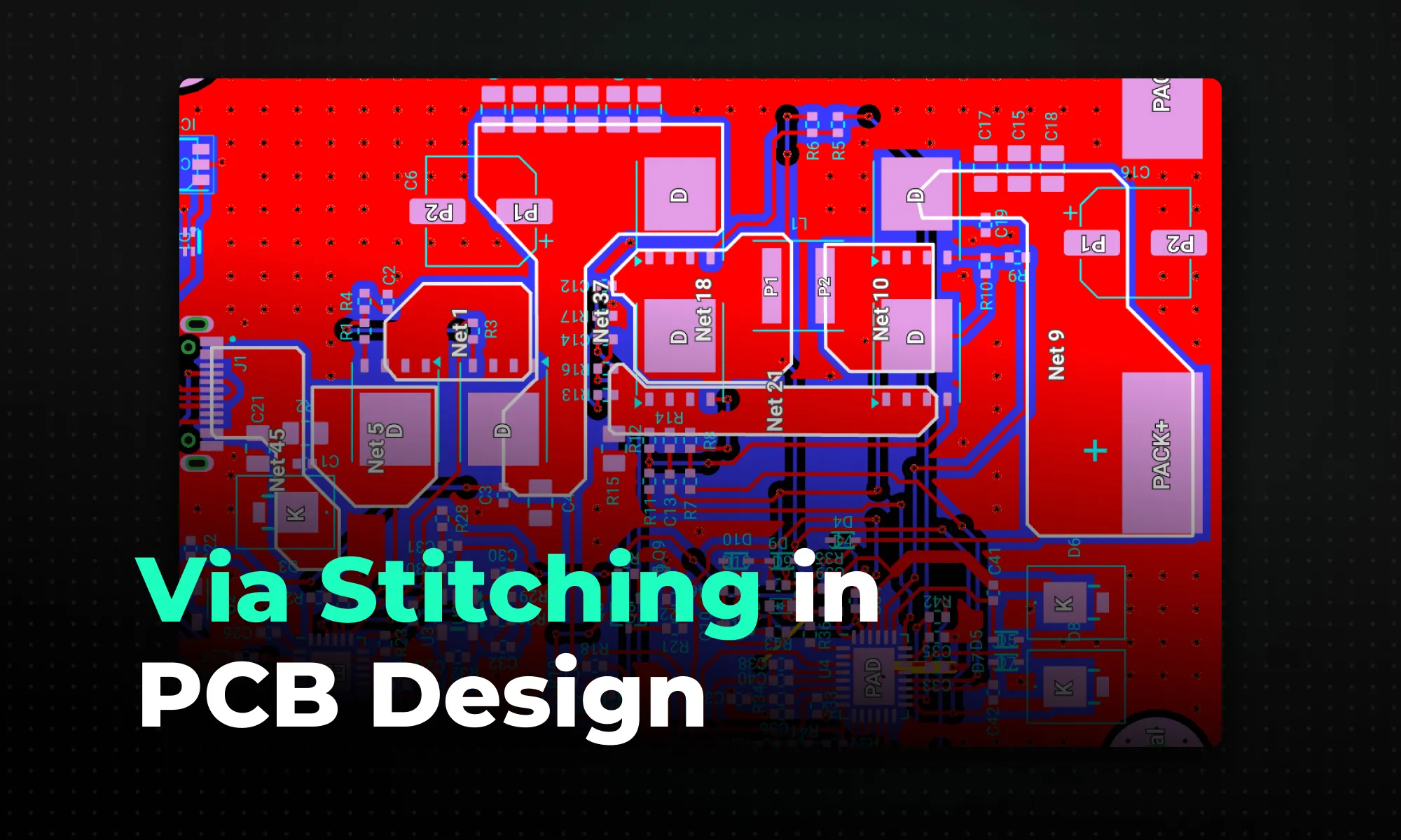
A practical guide to via stitching in PCB design -- what it is, why it improves EMI, signal integrity, and thermal performance, and where to place stitching vias. Includes spacing rules (like lambda/20), design guidelines, common mistakes to avoid, and how Flux can automate stitching via placement.
A guide to PCB component selection, covering electrical specs, footprints, thermal performance, sourcing, and best practices for picking parts that ship reliably.

A guide to PCB design reviews, covering schematic, layout, and DFM checks engineers use to catch errors early and ship more reliable boards.

A guide to creating and managing PCB footprint libraries, covering IPC standards, pad sizing, validation workflows, and best practices for reliable land patterns.

A guide to PCB schematic best practices, covering organization, symbols, labeling, and readability tips for clean, maintainable circuit diagrams.

A guide to flexible PCB design, covering materials, stackups, bend radius, and layout best practices for wearables, medical devices, and other compact electronics.

A beginner-friendly guide to reading PCB schematics, covering common symbols, nets, and how to follow signal flow through a circuit diagram.

An overview of collaborative PCB design, showing how cloud-native tools, real-time editing, and shared libraries are reshaping modern hardware team workflows.
