April 16, 2026
PCB Design for Manufacturability (DFM): Rules and Best Practices
Share

A printed circuit board (PCB) that functions flawlessly in a digital simulation is useless if a fabrication house cannot physically build it. Bridging the gap between the theoretical schematic and the physical production line requires adherence to PCB Design for Manufacturability (DFM).
DFM is the practice of designing your board to be manufacturable based on the physical capabilities and tolerances of modern manufacturing equipment. Failing to follow DFM guidelines results in expensive board re-spins, delayed product launches, and high defect rates. This guide breaks down the core DFM principles, common production pitfalls, and the exact rules you need to follow to ensure your layout is ready for the factory floor.
DFM stands for Design for Manufacturability. In the context of hardware engineering, it is the process of optimizing your PCB layout so that it can be fabricated and assembled as easily, reliably, and cost-effectively as possible.
While you might be able to draw a 2-mil (0.05mm) trace in your CAD software, a standard manufacturer's etching process might over-etch and dissolve that trace entirely, creating a broken circuit. PCB DFM involves understanding the physical and chemical limits of the circuit board production process, from copper etching and mechanical drilling to robotic pick-and-place assembly, and applying those limits to your layout as PCB design constraints.
Ignoring design for manufacturability PCB principles has severe financial and operational consequences.
To ensure a smooth transition from design to production, engineers must adhere to standard PCB manufacturing guidelines. Before starting a layout, always check your specific manufacturer's capabilities sheet.
Manufacturers have limits on how thin a trace can be and how close two traces can sit (often referred to as "trace/space"). A standard cost-effective rule is 6/6 mil (6 mil trace width, 6 mil spacing), while advanced high-density boards might push to 4/4 mil or 3/3 mil.
Drill bits have physical limits. A key metric is the aspect ratio (the board thickness divided by the drilled hole size). A safe industry standard is a 10:1 aspect ratio. Additionally, you must ensure a sufficient annular ring (the ring of copper surrounding the drilled hole) so that if the drill bit wanders slightly during manufacturing, it doesn't break outside the copper pad.
Component spacing prevents pick-and-place machine nozzles from knocking adjacent parts during assembly. It also ensures ensures there’s enough room for soldering irons or rework tools to access the pins.
Solder mask requires a slight expansion around copper pads to account for registration tolerances (misalignment during printing). If the expansion is too small, the soldermask might cover the pad, preventing solder from sticking. Furthermore, maintain a minimum "web width" of solder mask between closely spaced pads to prevent solder from bridging them together during reflow.
Even experienced engineers can overlook physical constraints. To help you identify risks during your layout phase, here is a breakdown of the most common PCB production issues caught during DFM reviews:
To avoid the PCB DFM errors mentioned above, run through this DFM PCB checklist before generating your manufacturing files:
These two terms are often used together, but they serve different purposes in the PCB layout for manufacturing workflow:
Historically, DFM was a disjointed process. Engineers would finish a layout, export the files, email them to a manufacturer, and wait days for a DFM report to come back filled with errors.
Modern, cloud-native platforms like Flux eliminate this friction by integrating PCB manufacturability rules directly into the design phase.
By utilizing real-time DRC, Flux prevents designers from making unmanufacturable routing decisions the moment they occur. If you attempt to place a via with an insufficient annular ring, the software flags it instantly. Furthermore, because Flux is a collaborative, browser-based platform, engineers can invite manufacturing partners directly into the design file for collaborative design reviews. Instead of emailing ZIP files back and forth, the fab house can highlight a problematic trace directly on the canvas, drastically accelerating the iteration cycle and ensuring the board is ready for flawless production on day one.


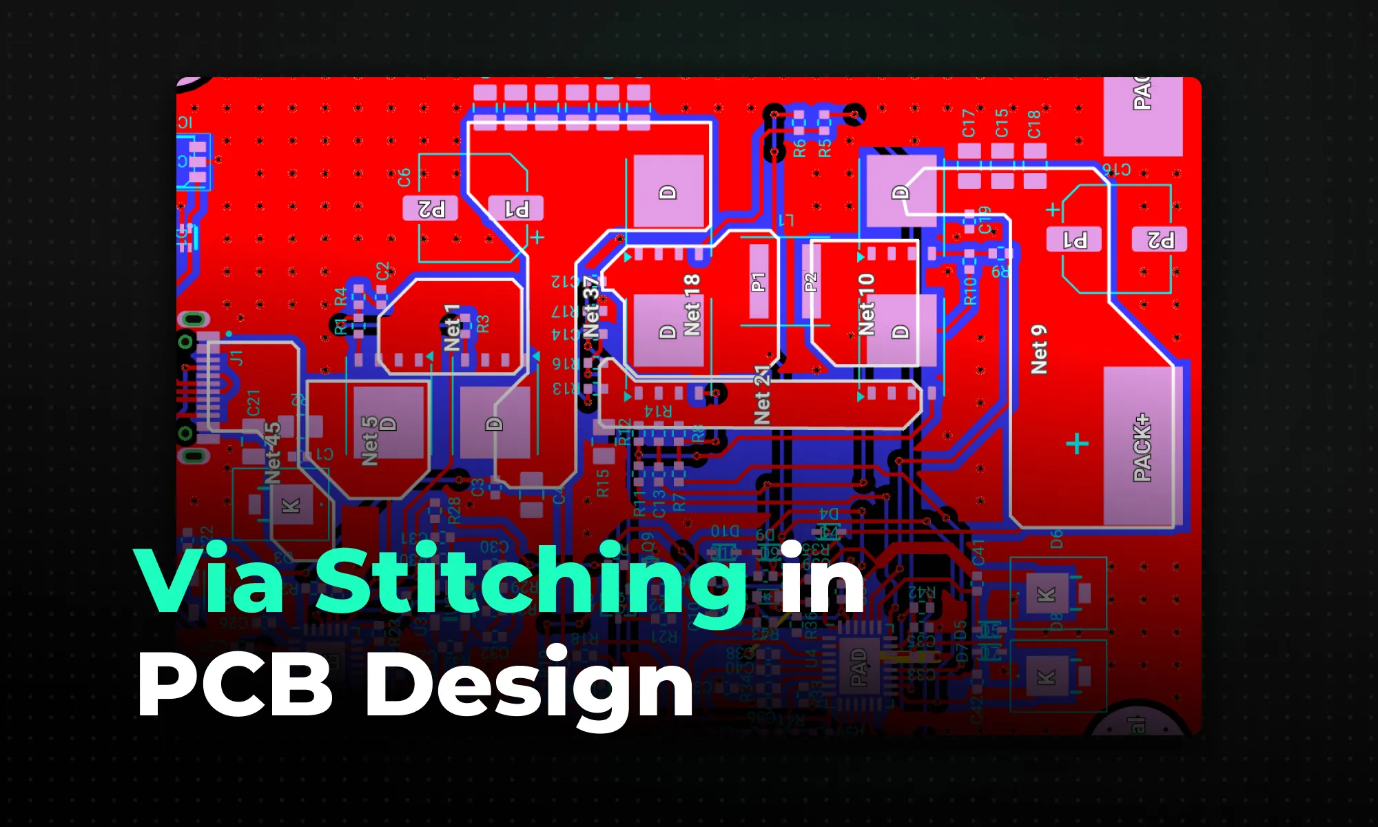
A practical guide to via stitching in PCB design -- what it is, why it improves EMI, signal integrity, and thermal performance, and where to place stitching vias. Includes spacing rules (like lambda/20), design guidelines, common mistakes to avoid, and how Flux can automate stitching via placement.
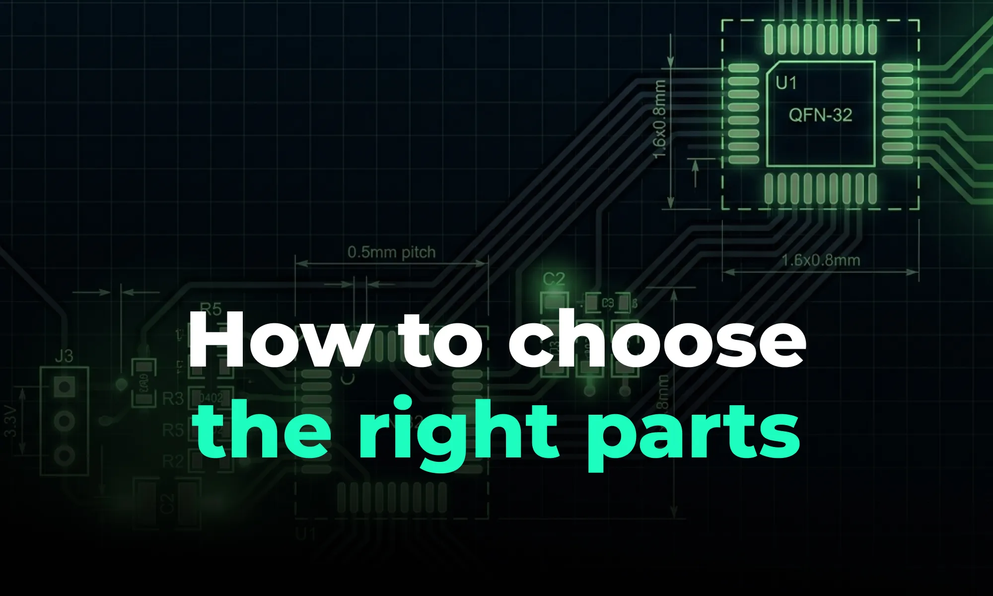
A guide to PCB component selection, covering electrical specs, footprints, thermal performance, sourcing, and best practices for picking parts that ship reliably.

A guide to PCB design reviews, covering schematic, layout, and DFM checks engineers use to catch errors early and ship more reliable boards.

A guide to creating and managing PCB footprint libraries, covering IPC standards, pad sizing, validation workflows, and best practices for reliable land patterns.

A guide to PCB schematic best practices, covering organization, symbols, labeling, and readability tips for clean, maintainable circuit diagrams.

A guide to flexible PCB design, covering materials, stackups, bend radius, and layout best practices for wearables, medical devices, and other compact electronics.

A beginner-friendly guide to reading PCB schematics, covering common symbols, nets, and how to follow signal flow through a circuit diagram.

An overview of collaborative PCB design, showing how cloud-native tools, real-time editing, and shared libraries are reshaping modern hardware team workflows.
