March 26, 2026
Design Rule Checking (DRC) in PCB Design: Real-Time vs Batch, Rules, and Common Failures
Share

In the world of electronics engineering, a printed circuit board might look perfect on your screen but be physically impossible to manufacture. A trace placed just a fraction of a millimeter too close to a via, or a drill hole sized slightly below the fabricator's capabilities, can result in short circuits, fabrication delays, and costly board re-spins.
This is where PCB design rule checks (DRC) becomes the safety net of the hardware development lifecycle. DRC acts as an automated auditor that verifies that your layout strictly adheres to both electrical requirements and the physical limits of your chosen manufacturer.
Design Rule Checking (DRC) is an automated verification process within Electronic Design Automation (EDA) software that ensures a circuit board layout complies with a predefined set of geometrical and electrical constraints.
Before a board is sent to a manufacturer, it must pass a PCB design rule check (DRC), which ensures the design complies with the manufacturer’s physical limitations in etching, drilling, and routing. For example, a standard fabrication house might have a minimum manufacturing tolerance of a 4-mil trace width and a 4-mil spacing gap. If you design a board with 3-mil traces, the manufacturer physically cannot produce it reliably.
By configuring your PCB manufacturing design rules upfront, DRC constantly scans the layout to catch errors, ensuring that elements like trace widths, copper clearances, and via geometries are safely within manufacturable limits. Catching a clearance violation in software costs nothing; finding out about it after ordering a batch of 500 boards is a costly disaster.
To effectively design a layout, engineers must configure various categories of PCB design rules. These constraints are typically derived from industry standards (like IPC-2221) and the specific capabilities of your chosen manufacturer.
The most common rule categories include:
Before beginning your layout or running a final check, verify you have configured constraints for:
Historically, PCB layout rule checks were handled as an afterthought. Today, modern workflows have shifted how these checks are executed.
In legacy desktop EDA tools, engineers typically route large sections of the board—or even finish the entire layout—before manually clicking a "Run DRC" button. This is known as Batch DRC.
The problem with batch DRC: Running a batch DRC at the end of a design phase often results in a massive, overwhelming list of hundreds of errors. Fixing a trace spacing issue found via a batch check might require you to rip up and reroute a massive section of a dense board, wasting hours of engineering time.
Modern PCB design platforms employ Real-Time DRC (or online DRC). In such a workflow, the software's rules engine runs constantly in the background.
The advantage of real-time DRC: Errors are detected during the layout process. If you attempt to draw a trace too close to a via, the software instantly flags the violation visually or actively prevents you from placing the invalid segment. This immediate feedback prevents errors from cascading, drastically reducing design iteration time and eliminating the dreaded "end-of-project error log."
Even with meticulous planning, engineers frequently encounter design rule check (DRC) violations during PCB layout. These errors typically occur when the physical layout conflicts with electrical or manufacturing constraints defined in the design rules. Recognizing the most common violations helps engineers identify and resolve problems quickly before manufacturing. Such common violations include trace clearance issues, overlapping copper features, incorrect trace widths, via aspect ratio problems, and component spacing conflicts.
The ultimate goal of a design rule check PCB workflow is bridging the gap between digital theory and physical manufacturing. By rigorously enforcing rules, DRC ensures:
(For deeper insights on planning highly reliable boards, explore our multilayer PCB design tutorial.)
Traditional EDA tools often treat design validation as a slow, batch-processed hurdle at the end of a project. Modern, cloud-native platforms like Flux flip this script by weaving validation directly into the active drafting process. By shifting from reactive troubleshooting to proactive guidance, modern tools improve the DRC workflow in several key ways.
Ultimately, this combination of real-time feedback and collaboration reduces the risk of costly manufacturing errors. By ensuring every routing decision complies with fabrication limits the moment it is made, modern platforms prevent unmanufacturable designs from ever reaching the fab house, eliminating unnecessary board re-spins and maintaining tight project schedules.


A guide to flexible PCB design, covering materials, stackups, bend radius, and layout best practices for wearables, medical devices, and other compact electronics.

A beginner-friendly guide to reading PCB schematics, covering common symbols, nets, and how to follow signal flow through a circuit diagram.

Learn the key differences between analog and digital PCB design and how to manage mixed-signal layouts for better signal integrity.

Learn how to place and select decoupling capacitors to improve power integrity in PCB design.
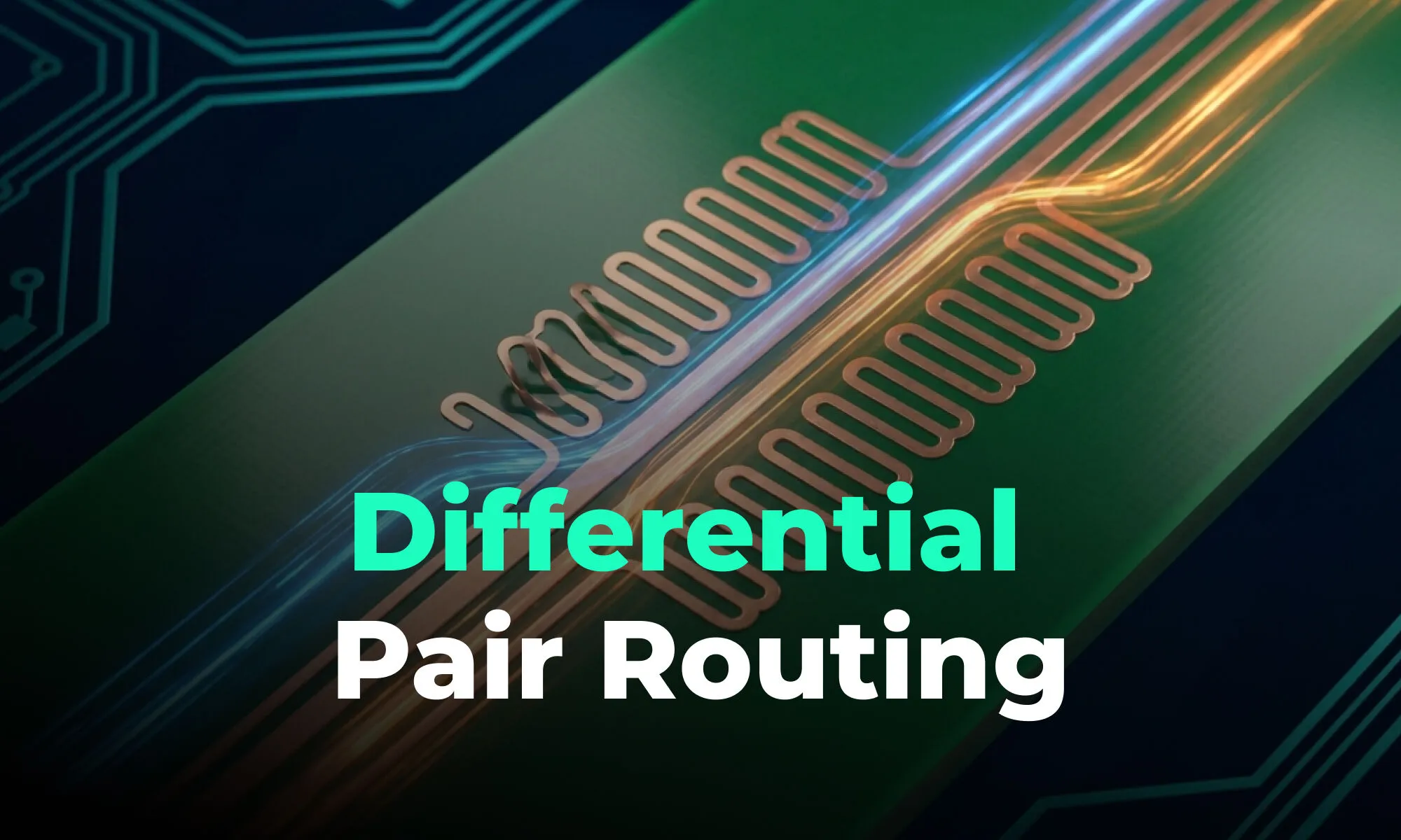
Learn the core rules of differential pair routing including parallel routing, consistent spacing, length matching, and return path management for high-speed PCB designs.

Learn the most common causes of PCB EMI issues and proven layout, grounding, shielding, and filtering techniques to pass EMC compliance.

Learn the most common PCB testing methods including flying probe and in-circuit testing to ensure reliability.

Learn how to manage heat in PCB design with thermal vias, copper pours, layout strategies, and cooling techniques to improve reliability.
