As a design moves from a single prototype to mass production, handling individual boards one at a time quickly becomes inefficient. Fabrication houses don't process PCBs individually, they work with large, standardized sheets of material. To make use of that space efficiently, designers and manufacturers group multiple boards together using a process called PCB panelization.

This process involves grouping multiple small boards into a larger "array" or "panel." By treating the group as a single unit, machines can place components and move the boards through the assembly line at much higher speeds. This guide covers the methods and design rules for creating a manufacturing-ready panel.

Key Takeaways

What Is PCB Panelization?

PCB panelization is the technique of arranging multiple PCBs onto a single, larger substrate for the purpose of streamlined manufacturing. This resulting assembly is often also called a PCB array design.

While you might only need ten boards for a prototype run, a production order for ten thousand units requires a high-level approach to PCB production efficiency. The panel typically includes "waste" material around the edges, known as rails or break-away tabs, which provide the conveyor belts and robotic arms material to grip during the soldering and pick-and-place stages.

Why Panelization Is Important

Panelization is a core part of PCB manufacturing optimization. Without it, the cost of high-volume production would be prohibitive.

  • Cost Reduction: By fitting as many boards as possible onto a standard production panel, you reduce material waste. You pay for the area of the large sheet; leaving it empty increases the cost per unit.
  • Manufacturing Throughput: Assembly machines can place components on twelve boards in a single panel faster than they can process twelve individual boards.
  • Standardization: Panels allow small, oddly shaped boards to fit into standard assembly equipment that expects a certain minimum size.

Common PCB Panelization Methods

There are two primary ways to connect boards within an array so they stay together during assembly but can be separated afterward.

Method Description Best For Pros Cons
V-scoring PCB A triangular groove is cut into the top and bottom of the board, leaving a thin web of material. Rectangular or square boards. Maximum material usage; very fast separation. Only works for straight lines; can leave rough edges.
Tab Routing PCB The board outline is fully cut, leaving small copper-less bridges (tabs) to hold it to the frame. Irregular, circular, or complex board shapes. High precision; handles any shape. Wastes more material; tabs require manual or machine cleanup.

Panel Design Best Practices

Designing a successful PCB panel design requires balancing the need for easy separation with the need for mechanical stability.

  • Maintain Structural Integrity: If a panel is too flimsy, it will sag in the reflow oven. Use wide enough rails (typically 5mm to 10mm) to keep the array flat. Board orientation should also align the mechanically stronger axis with conveyor travel to reduce flex.
  • Component Clearance: Keep sensitive components (like ceramic capacitors) at least 3mm to 5mm away from the V-score or tabs. The mechanical stress of breaking the boards apart can crack small components.
  • Tooling Holes: Add non-plated holes (usually 3.175mm) in the corners of the panel rails. These allow the assembly machines to align the panel accurately.
  • Fiducial Marks: Place global fiducials on the panel rails to help the pick-and-place cameras find the exact orientation of the array.

Common Panelization Mistakes

  • Ignoring Overhanging Components: Connectors that stick out past the board edge will collide with adjacent boards in a panel if the spacing is not wide enough.
  • Weak Tab Placement: Placing too few tabs can cause the board to fall out of the panel during assembly. Placing too many makes depanelization difficult and increases the risk of board damage.
  • Inconsistent Scoring Depth: If the V-score is too deep, the board is fragile. If it is too shallow, the force required to break it will be so high that you risk snapping the board or delaminating the traces.

How Panelization Impacts Cost and Production

Panel utilization directly affects fabrication cost. Higher material utilization improves manufacturing efficiency and lowers per-board cost, especially for high-layer-count designs.

The depanelization method also affects production cost and yield:

  • V-scoring is lower cost and faster but limited to straight edges and introduces higher mechanical stress.
  • Tab routing supports irregular geometries and reduces stress but increases CNC routing time and requires mouse-bite cleanup.

Well-optimized panel layouts improve assembly throughput, reduce scrap rates, and minimize mechanical failures during manufacturing.

How Modern PCB Tools Help

Setting up a panel manually can be a tedious process of calculating X and Y offsets. Modern platforms like Flux simplify this by providing collaborative environments where manufacturing requirements are integrated into the design flow.

Because Flux is browser-based, you can invite your fabrication partner directly into the project. They can provide immediate feedback on the PCB array design, ensuring the tooling holes and rails meet their machine specifications before you finalize the order. This real-time validation prevents the "back-and-forth" emails that often delay production and ensures your design is ready for high-yield manufacturing from the start.

Move from manual panel calculations to real-time collaborative manufacturing feedback, start your next PCB panel in Flux and get fabrication-ready faster.

FAQs

What are "mouse bites" in PCB design?
Mouse bites are a series of small holes drilled into a routing tab. They act like a perforated line on a sheet of paper, making it easier to break the board away from the panel frame.
When should I use V-scoring vs. tab routing?
Use V-scoring if your boards are rectangular and can be separated by a straight cut. Use tab routing if your boards have curves or if components are placed too close to the edge to survive the stress of V-scoring.
Does panelization affect signal integrity?
Generally, no. Since the rails and tabs are removed after assembly, they do not impact the final electrical performance. However, you must ensure that copper traces do not run through the V-score areas.
What is depanelization?
Depanelization is the final step in the PCB manufacturing optimization process where individual boards are removed from the array. This can be done by hand, with a pizza-cutter-style blade, or a robotic router.
Can I panelize different designs on the same panel?
Yes, this is called "prototype panelization" or "multitasking." It is a great way to save money when you need a few copies of several different designs.
Profile avatar of the blog author

Yaneev Hacohen

Yaneev Cohen is an electrical engineer concentrating in analog circuitry and medical devices. He has a Master's and Bachelor's in Electrical Engineering and has previously worked for Cadence and Synopsys's technical content departments.

Go 10x faster from idea to PCB
Work with Flux like an engineering intern—automating the grunt work, learning your standards, explaining its decisions, and checking in for feedback at key moments.
Illustration of sub-layout. Several groups of parts and traces hover above a layout.
Design PCBs with AI
Introducing a new way to work: Give Flux a job and it plans, explains, and executes workflows inside a full browser-based eCAD you can edit anytime.
Screenshot of the Flux app showing a PCB in 3D mode with collaborative cursors, a comment thread pinned on the canvas, and live pricing and availability for a part on the board.

Related Content

How to Use Via Stitching in PCB Design

How to Use Via Stitching in PCB Design

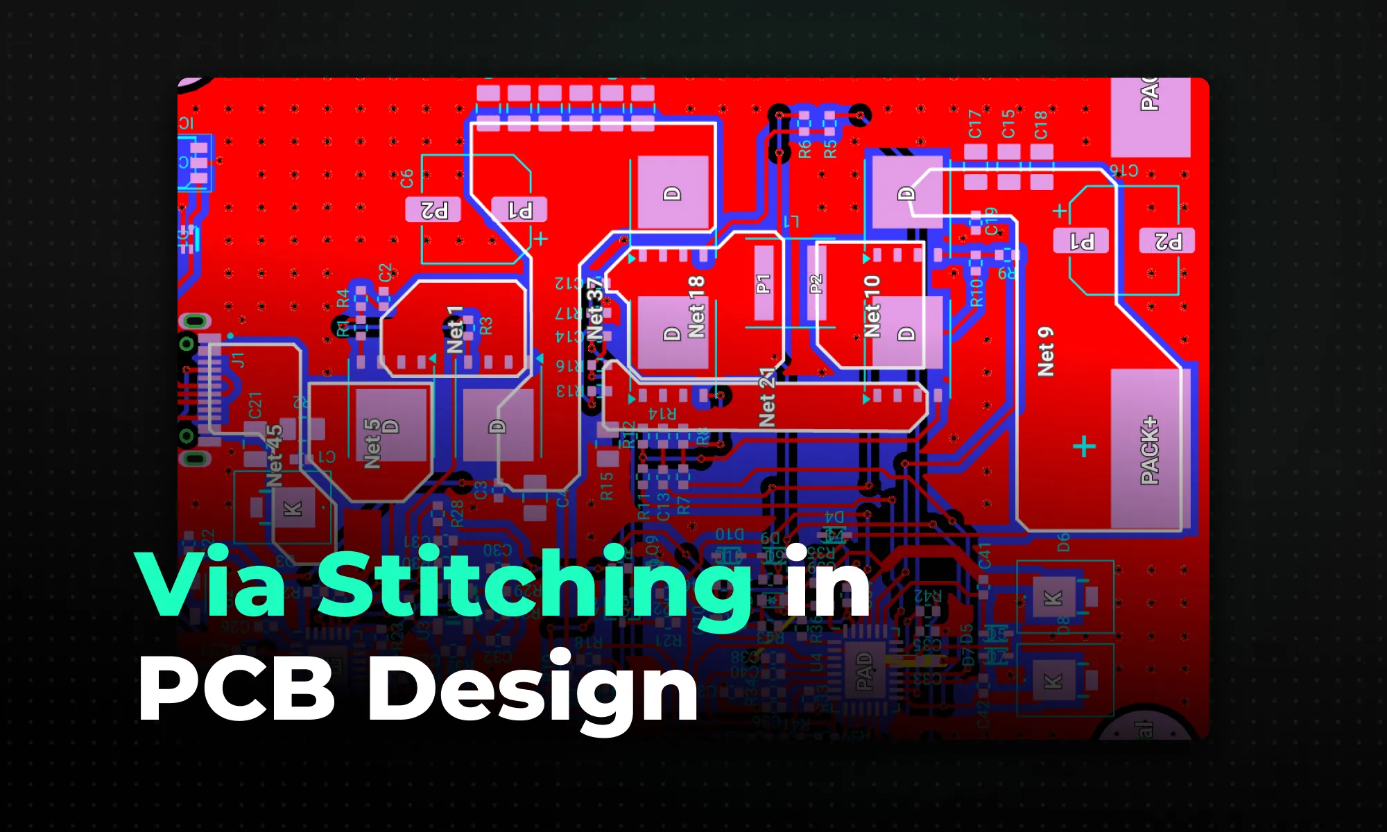
A practical guide to via stitching in PCB design -- what it is, why it improves EMI, signal integrity, and thermal performance, and where to place stitching vias. Includes spacing rules (like lambda/20), design guidelines, common mistakes to avoid, and how Flux can automate stitching via placement.

Profile avatar of Yaneev Hacohen
Yaneev Hacohen
|June 24, 2026
Component Selection in PCB Design: How Engineers Choose the Right Parts

Component Selection in PCB Design: How Engineers Choose the Right Parts

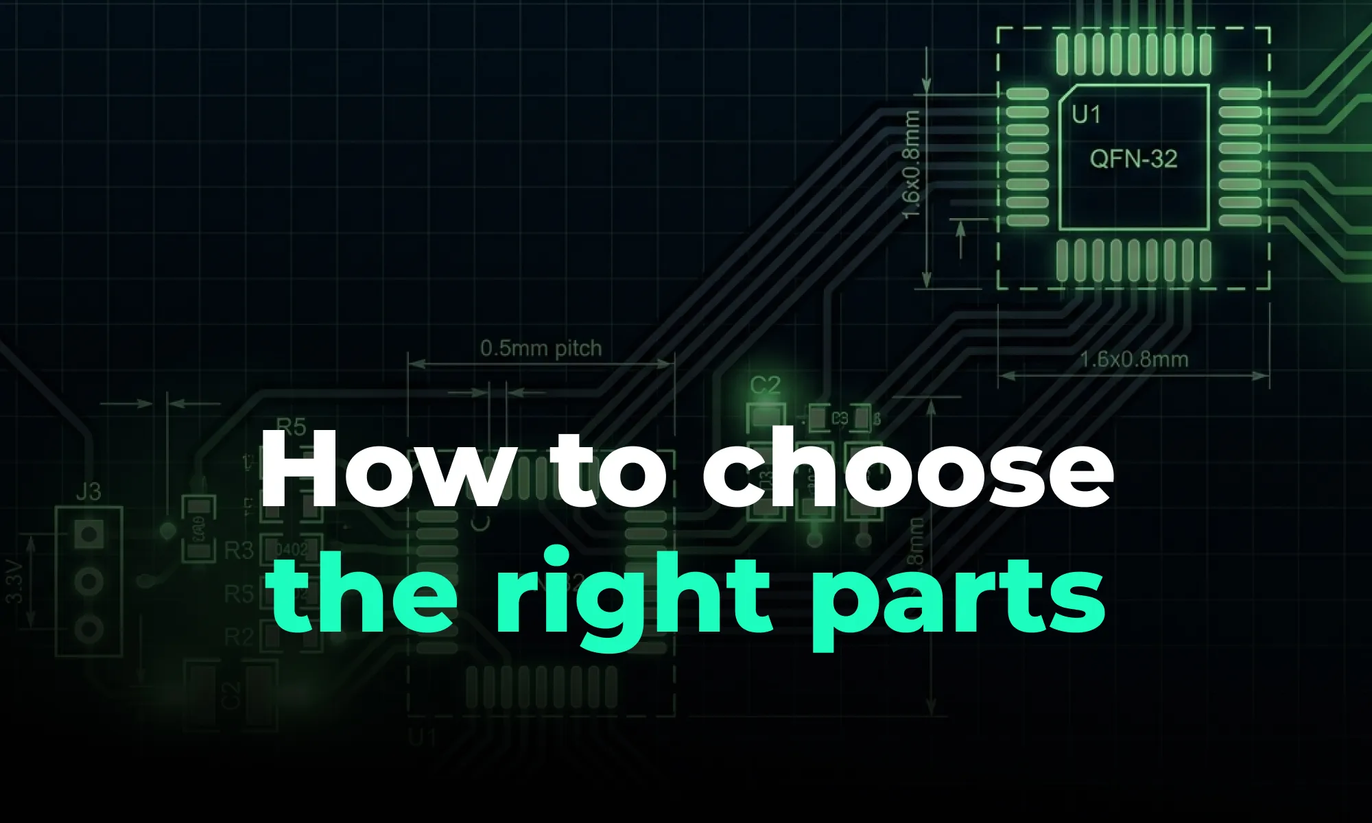
A guide to PCB component selection, covering electrical specs, footprints, thermal performance, sourcing, and best practices for picking parts that ship reliably.

Profile avatar of Yaneev Hacohen
Yaneev Hacohen
|June 15, 2026
PCB Design Reviews: Best Practices for Catching Errors Early

PCB Design Reviews: Best Practices for Catching Errors Early

A guide to PCB design reviews, covering schematic, layout, and DFM checks engineers use to catch errors early and ship more reliable boards.

Profile avatar of Yaneev Hacohen
Yaneev Hacohen
|June 15, 2026
How to Create and Manage PCB Footprint Libraries

How to Create and Manage PCB Footprint Libraries

A guide to creating and managing PCB footprint libraries, covering IPC standards, pad sizing, validation workflows, and best practices for reliable land patterns.

Profile avatar of Yaneev Hacohen
Yaneev Hacohen
|June 15, 2026
PCB Schematic Best Practices for Clean Circuit Design

PCB Schematic Best Practices for Clean Circuit Design

A guide to PCB schematic best practices, covering organization, symbols, labeling, and readability tips for clean, maintainable circuit diagrams.

Profile avatar of Yaneev Hacohen
Yaneev Hacohen
|June 15, 2026
Flexible PCB Design Guide: Materials, Layout, and Applications

Flexible PCB Design Guide: Materials, Layout, and Applications

A guide to flexible PCB design, covering materials, stackups, bend radius, and layout best practices for wearables, medical devices, and other compact electronics.

Profile avatar of Yaneev Hacohen
Yaneev Hacohen
|June 8, 2026
How to Read PCB Schematics: A Beginner-Friendly Guide

How to Read PCB Schematics: A Beginner-Friendly Guide

A beginner-friendly guide to reading PCB schematics, covering common symbols, nets, and how to follow signal flow through a circuit diagram.

Profile avatar of Yaneev Hacohen
Yaneev Hacohen
|June 8, 2026
Collaborative PCB Design: Why Hardware Teams Are Moving to the Cloud

Collaborative PCB Design: Why Hardware Teams Are Moving to the Cloud

An overview of collaborative PCB design, showing how cloud-native tools, real-time editing, and shared libraries are reshaping modern hardware team workflows.

Profile avatar of Yaneev Hacohen
Yaneev Hacohen
|June 5, 2026