September 18, 2023
Understanding the Flyback Diode: Your Essential Guide to Functionality and Why You Need One
Share


A flyback diode is a semiconductor device that is connected across an inductor in a circuit to protect other components from voltage spikes. When an inductive load is suddenly de-energized, the energy stored in the inductor has to go somewhere. The flyback diode provides a path for this energy, preventing damage to other components like transistors.
Inductors store energy in their magnetic fields. When the current flowing through an inductor changes, it induces an electromotive force (EMF) due to its inductance. This induced EMF can be harmful to other components in the circuit, especially sensitive ones like integrated circuits (ICs).
When an inductive load like a solenoid or coil is switched off, the energy stored in its inductance must be dissipated. Without a flyback diode, this energy can cause voltage spikes, leading to arcing across switch contacts and potential damage to ICs.
Transistors are particularly vulnerable to voltage spikes. A flyback diode can protect the transistor by providing a path for the inductive energy to be safely dissipated.
In some applications, a resistor or a snubber circuit may be used in conjunction with the flyback diode to dampen oscillations and further protect the circuit.
Understanding the flyback diode is crucial for anyone dealing with circuits that include inductive elements. Whether you're working with solenoids, coils, or any inductive load, a flyback diode is your go-to component for protecting against voltage spikes and ensuring that energy is safely dissipated. By selecting the appropriate type—be it a standard, Zener, or freewheeling diode—you can optimize your circuit for both safety and efficiency.


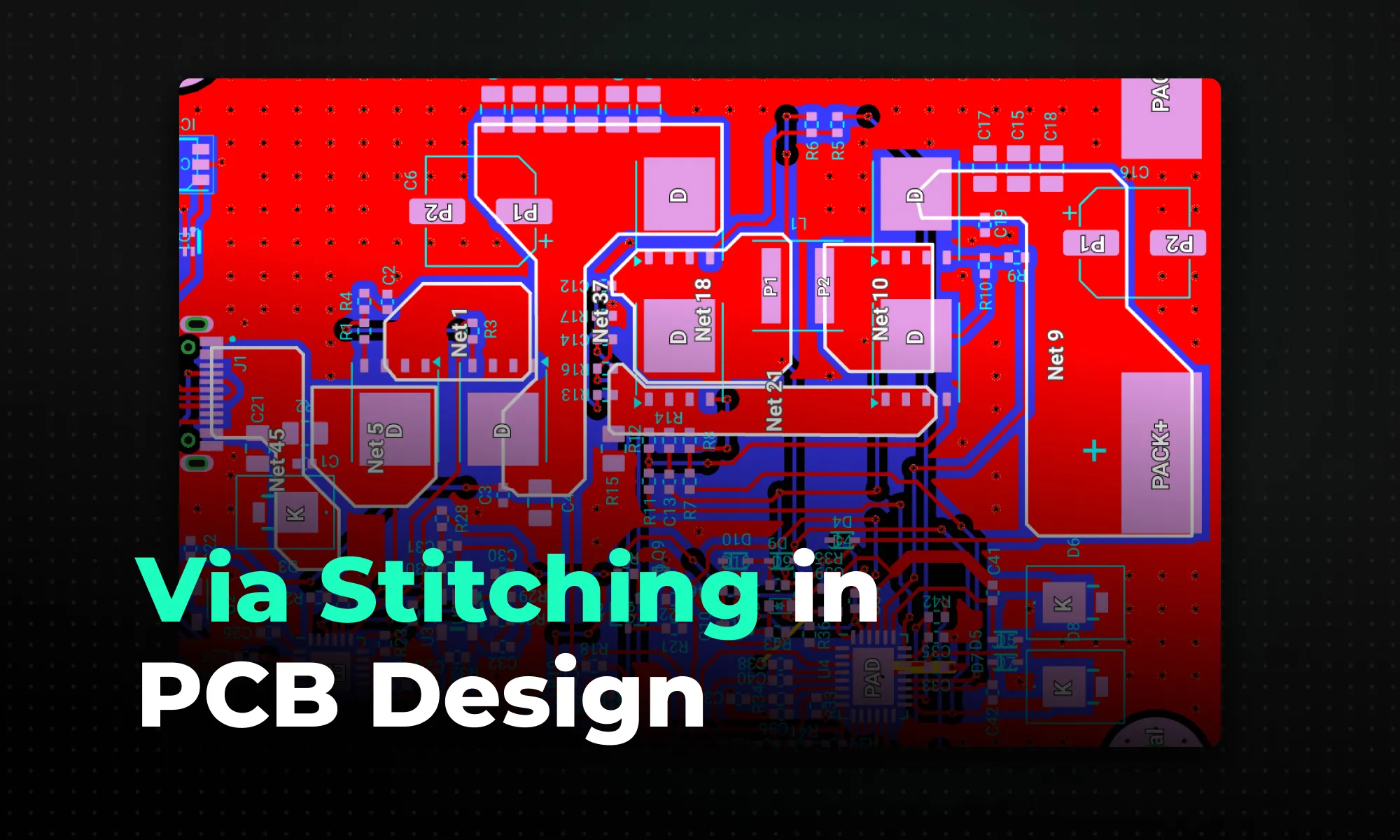
A practical guide to via stitching in PCB design -- what it is, why it improves EMI, signal integrity, and thermal performance, and where to place stitching vias. Includes spacing rules (like lambda/20), design guidelines, common mistakes to avoid, and how Flux can automate stitching via placement.
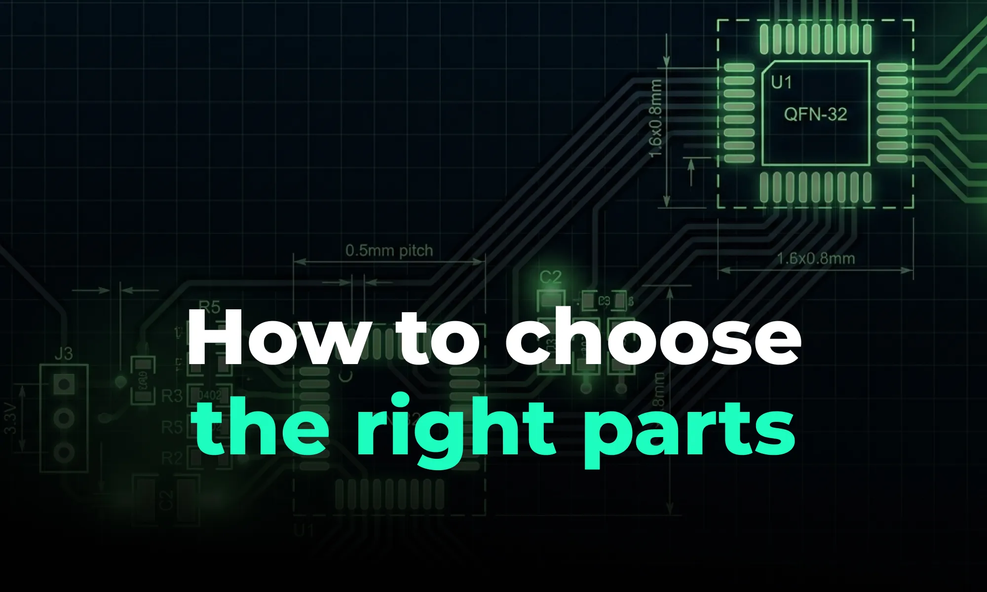
A guide to PCB component selection, covering electrical specs, footprints, thermal performance, sourcing, and best practices for picking parts that ship reliably.

A guide to PCB design reviews, covering schematic, layout, and DFM checks engineers use to catch errors early and ship more reliable boards.

A guide to creating and managing PCB footprint libraries, covering IPC standards, pad sizing, validation workflows, and best practices for reliable land patterns.

A guide to PCB schematic best practices, covering organization, symbols, labeling, and readability tips for clean, maintainable circuit diagrams.

A guide to flexible PCB design, covering materials, stackups, bend radius, and layout best practices for wearables, medical devices, and other compact electronics.

A beginner-friendly guide to reading PCB schematics, covering common symbols, nets, and how to follow signal flow through a circuit diagram.

An overview of collaborative PCB design, showing how cloud-native tools, real-time editing, and shared libraries are reshaping modern hardware team workflows.
