Today’s complex PCB designs are more challenging than ever before due to fast signal speeds. Knowing and implementing the industry’s PCB design best practices is the key!

All electronic devices and circuits produce excess heat, necessitating effective thermal management to enhance reliability and avoid early failure. The heat output equals the power input, assuming no other energy interactions. Various cooling techniques are used, such as different types of heat sinks, thermoelectric coolers, forced air systems and fans, heat pipes, and thermal management on PCB layout level.

Electric currents generate heat as they pass through resistive elements of a circuit. The higher the resistance of a conductor, the more heat will be generated as current passes through it. Therefore, addressing both electric and thermal parameters in board design is essential for long-term functionality. PCB thermal analysis plays a vital role in the design process, as it can predict thermal flaws and provide an opportunity for circuit redesign. Some key PCB design considerations for improved thermal performance include temperature-sensitive components. Components that are especially sensitive to temperature should be placed in the location with the lowest temperature, such as the bottom of the board.

The simplest way to dissipate heat would be through thermal vias to the cooling system (heat sink or heat pipes). The heat sink draws heat away from the PCB to fins that provide a larger surface area for faster heat dissipation.

PCB Thermal Analysis Basics

Thermal Equivalent Circuits

Thermal Equivalent Circuits are an analogy of electrical circuits to provide an estimation of the flow of heat in a design. They work because the underlying equations for the transfer of thermal energy and electrical energy are similar enough. With the analogies, we can calculate the heat transfer within the PCB.

Thermal Equivalent Analogy of Electrical Circuits

Electrical Circuit Thermal Equivalent
Current (A) Heat flow (W)
Voltage drop (V) Junction temperature (°C)
Electrical resistance (Ohm) Thermal resistance (°C/W)
Capacitance (F) Heat capacity (J/°C)

Equivalent Equations

I = V1-V2/R => Q = T1-T2/Rt

Where:
I is the current (A)
V is the voltage (V)
R is the electrical resistance
Q is the heat flow (W)
T is the junction temperature (°C)
Rt is the thermal resistance (°C/W)

Similarly, equivalent thermal resistance in series and parallel also follows the same equations for electrical resistance.

Component Thermal Impedance

Thermal impedance measures the sum of thermal resistance and thermal contact resistance of a material. This value can be found in the component datasheet for integrated circuits and ranges from 20 °C/W for low-power amplifiers or ICs, to as high as ~200 °C/W for powerful microprocessors. The operating temperature can be determined by multiplying the component’s power consumption by its thermal impedance.

T = Z*P

Where:
T is the component temperature (°C).
P is the power usage of the component (W)
Z is the thermal impedance (°C/W)

Thermal Management Considerations

  • Materials and Temperature Ratings
  • Use PCB substrate material with appropriate ratings for your operating environment.
  • FR-4, the most common PCB material, is rated to operate up to 130 degrees.
  • Consider alternatives like Shengyi S1000-2 or ARLON 85N for higher temperature operations.

Increasing Thermal Conductivity

When your PCB generates significant heat, choosing a substrate with superior thermal conductivity is crucial. Ceramics are an excellent option due to their high thermal conductivity and adjustable mechanical properties, which help manage mechanical stress during thermal cycling. Adding a metal core to the board or increasing copper below components, such as adding a plane layer, can also enhance heat dissipation.

When designing PCBs, the importance of effective thermal management cannot be overstated. High-power components generate significant heat, and without proper dissipation, the performance and longevity of the circuit boards can be compromised. One effective method to manage this heat is by using a heat sink. A heat sink helps to draw heat away from critical components, improving the overall thermal performance of the PCB.

Thermal relief is also design feature used in electronic circuit boards to manage heat dissipation from components that generate significant heat during operation. It helps to prevent overheating and ensures the reliability and longevity of the components.

Shows two types of thermal relief in a pcb layout
Learn more about Thermal Relief

There are two main configurations for thermal relief:

  1. Relief Connect: This option creates an air gap between the thermal pad and the fill material, connecting them with conductors. This configuration allows for some thermal isolation, which can be beneficial in certain applications where you want to limit heat transfer.
  2. Direct Connect: This option removes the air gap, allowing the thermal pad and the fill material to be in full contact. This configuration provides better thermal conductivity, which is ideal for components that need to dissipate heat quickly.

PCBs are the backbone of modern electronics, and ensuring they operate within safe thermal limits is crucial. Circuit boards that overheat can lead to component failure and reduced reliability. This is why thermal resistance and thermal impedance are important parameters to consider in PCB design. By carefully selecting materials and employing efficient cooling techniques, such as integrating cooling fans, the thermal performance of PCBs can be significantly enhanced.

Tips for Sensitive and High-Power Components

  • Place temperature-sensitive components in cooler areas, away from high-heat producers like frequency transistors and microprocessors.
  • Position passive components near the edges and high-powered ones in the center for even temperature distribution.
  • Spread high-power components out to prevent hotspots.
  • Use metal-plated holes and short leads for better heat transfer. Choose components with suitable temperature ratings and larger cross-sectional areas for efficient heat dissipation.
  • Use mounting screws to enhance thermal distribution.
  • Incorporate thermal vias with grounded polygon pours beneath heat-generating components.

Fan and Heat Sink Considerations

  • Thermal Interface Materials: Utilize thermal pads and pastes to enhance heat transfer from components to heat sinks or enclosure walls.
  • Fan Placement: Position fans directly on hot components for efficient cooling or mount larger fans on the enclosure for quieter and more energy-efficient heat removal.
  • Heat Sink Design: Customize heat sink designs for maximum convective cooling, ensuring they are compatible with the airflow provided by the fan placement.
  • Enclosure Integration: Attach the PCB directly to a metal enclosure with thermal interface material to enhance heat transfer to the surrounding environment.

Other Considerations for Routing Traces

  • Trace Design: Keep power traces short and wide to reduce heat generation. Round corners and avoid right angles to minimize inductance and noise.
  • Ground and Power Planes: Maximize the size of copper planes to act as heat sinks and connect them to external layers for improved heat transfer.
  • Thermal Vias: Use them to dissipate heat from multi-layer boards and internal copper layers.
  • Standards Compliance: Follow IPC, UL, and IEC standards for current density and conductor spacing to ensure thermal reliability.

PCB Thermal Simulation

PCB thermal simulation enables designers to predict thermal management issues, ensuring optimal heat dissipation. By simulating different layouts and thermal solutions, designers can avoid costly physical iterations and achieve a thermally efficient design from the outset.

Key advantages of PCB thermal simulation include the ability to

  • Identify thermal hotspots, thermal interferences
  • Analyze airflow, temperature distribution, heat dissipation and heat release patterns.
  • Evaluate the configuration of thermal vias
  • Assess the heat sink's performance and different cooling technique efficiency
  • Optimize the PCB layout cost-effectively.

Thermally conductive materials, such as certain ceramics, can greatly improve the heat dissipation capabilities of circuit boards. Additionally, incorporating thermal vias and using thermally conductive paste can further aid in managing the heat generated by high-power components. Cooling fans are another essential element in thermal management, ensuring that heat is effectively removed from the PCB and dissipated into the surrounding environment.

PCB design requires careful consideration of thermal management techniques. By utilizing heat sinks, thermally conductive materials, and cooling fans, designers can create circuit boards that operate efficiently and reliably, even under demanding conditions. Proper thermal analysis and simulation are key to achieving optimal performance and preventing overheating issues in PCBs.
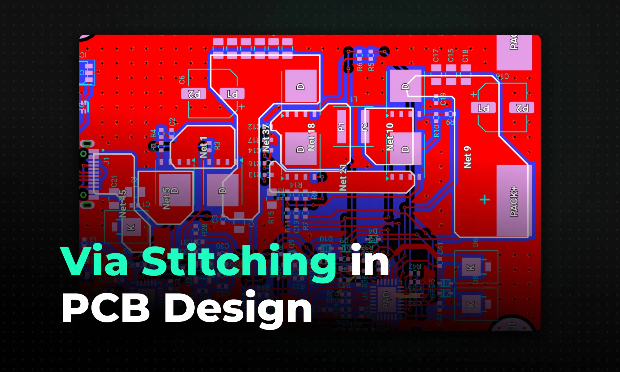
Profile avatar of the blog author

Jharwin Barrozo

Jharwin is an electronics engineer mainly focused on satellites. He built his own ground station using Flux to monitor RF activities on the International Space Station. Find him on Flux @jharwinbarrozo

Go 10x faster from idea to PCB
Work with Flux like an engineering intern—automating the grunt work, learning your standards, explaining its decisions, and checking in for feedback at key moments.
Illustration of sub-layout. Several groups of parts and traces hover above a layout.
Design PCBs with AI
Introducing a new way to work: Give Flux a job and it plans, explains, and executes workflows inside a full browser-based eCAD you can edit anytime.
Screenshot of the Flux app showing a PCB in 3D mode with collaborative cursors, a comment thread pinned on the canvas, and live pricing and availability for a part on the board.

Related Content

PCB Prototyping vs. Fabrication: Which Process Is Right for Your Project?

PCB Prototyping vs. Fabrication: Which Process Is Right for Your Project?

A practical guide to when hardware teams should use low-volume PCB prototyping to validate a design versus full-scale fabrication to scale production, and how to transition between the two without costly mistakes.

Profile avatar of Yaneev Hacohen
Yaneev Hacohen
|April 21, 2026
Blind Vias, Buried Vias, and Microvias: A Complete Guide to PCB Via Types

Blind Vias, Buried Vias, and Microvias: A Complete Guide to PCB Via Types

A practical guide to the four main PCB via types — through-hole, blind, buried, and microvia — covering how each is fabricated, their cost and signal-integrity trade-offs, and when to use them based on layer count, BGA pitch, and routing density.

Profile avatar of Yaneev Hacohen
Yaneev Hacohen
|April 21, 2026
PCB Design for Manufacturability (DFM): Rules and Best Practices

PCB Design for Manufacturability (DFM): Rules and Best Practices

Learn PCB design for manufacturability (DFM) guidelines, rules, and common issues to ensure your circuit boards can be reliably produced.

Profile avatar of Yaneev Hacohen
Yaneev Hacohen
|April 16, 2026
Best PCB Routing Techniques for Clean Circuit Board Layouts

Best PCB Routing Techniques for Clean Circuit Board Layouts

Learn the best PCB routing techniques for clean circuit board layouts, including trace routing tips, differential pair routing, and layout best practices.

Profile avatar of Yaneev Hacohen
Yaneev Hacohen
|April 16, 2026
High-Speed PCB Design: Layout Rules, Signal Integrity, and Routing Best Practices

High-Speed PCB Design: Layout Rules, Signal Integrity, and Routing Best Practices

Whether you're migrating from popular EDA applications or starting fresh, mastering high speed PCB design has never been more intuitive. Flux enables teams to design, simulate, and route with real-time AI assistance, so you can spin your next high-speed board with total confidence.

Profile avatar of Yaneev Hacohen
Yaneev Hacohen
|March 26, 2026
Design Rule Checking (DRC) in PCB Design: Real-Time vs Batch, Rules, and Common Failures

Design Rule Checking (DRC) in PCB Design: Real-Time vs Batch, Rules, and Common Failures

DRC is an automated process that checks your PCB layout against manufacturing and electrical constraints, catching errors like trace spacing and drill sizes before fabrication. Modern tools run this in real-time during design, while older ones batch-check at the end, often producing overwhelming error lists.

Profile avatar of Yaneev Hacohen
Yaneev Hacohen
|March 26, 2026
What Is a PCB? A Beginner's Guide to Printed Circuit Board Design

What Is a PCB? A Beginner's Guide to Printed Circuit Board Design

Whether you are exploring “What is a PCB?” for the first time or moving into advanced hardware engineering, modern tools make the process easier than ever. With Flux's AI-assisted platform, you can skip the steep learning curve of popular ECAD applications and design collaboratively directly in your browser. Once your board is routed and ready for fabrication, Flux's built-in supply chain features connect you directly with worldwide distributors to source parts instantly. Sign up for free today and start building!

Profile avatar of Yaneev Hacohen
Yaneev Hacohen
|March 21, 2026
Simulate Circuits with a Prompt

Simulate Circuits with a Prompt

Flux brings circuit simulation to wherever you are in the design process. Start from a prompt when you have no schematic, or let Flux analyze your existing design automatically.

Profile avatar of Lance Cassidy
Lance Cassidy
|March 20, 2026