When you think about what makes a board “good,” you probably picture sleek routing, component placement, maybe even signal integrity sims. But many of the most frustrating bugs—like unexpected EMI, power noise, or layout-dependent failures—trace back to something deeper: the way your board handles return paths.

That’s where ground planes, zones, and stackup symmetry come in. They’re the quiet guardians of signal integrity, and Flux is built to help you get them right—without the guesswork.

In this post, we’ll explore why these concepts matter, how they impact signal integrity and power distribution, and what to keep in mind as you design. If you want to go deeper into implementation details—like when to use zones, where to place stitching vias, or how to avoid stackup pitfalls—we’ve created a detailed PDF guide just for that.

The Hidden Hero of Every Signal

Every signal you route is part of a circuit. And that circuit includes the return path—the signal that flows back to the source. At high speeds, this return doesn't just wander through your board—it seeks the lowest impedance path back.

That path is normally the ground plane directly beneath the signal layer. If the plane is continuous, the return path stays tight, inductance stays low, and EMI stays minimal.

But if the ground is broken—say, by a split—the return path will form a bigger loop. And bigger loops might mean bigger problems: signal distortion and radiated emissions that could cause a failed EMI test.

Good return paths are invisible when they work, and painfully visible when they don’t.

The Great Ground Plane Debate

You’ve probably heard the advice: “Split your ground plane between analog and digital.” Sometimes that’s sound engineering. But often, it leads to more trouble than it solves.

The key question isn’t “Should I split my ground plane?”—it’s “Will this split create more noise than it prevents?”

In most cases, you should avoid splitting the ground plane. Here's why:

  • Every signal needs a return path. And the lowest-impedance return path is usually the plane directly beneath the signal trace.
  • When that plane is continuous, return currents flow tightly under the signal, minimizing loop area and reducing EMI.
  • If you introduce a split, return currents are forced to detour around it—expanding the loop area and increasing inductive coupling and noise.
  • You can also end up with isolated copper regions that act as unintended antennas or pick up stray currents.
  • Here’s a good example of a 4-layer board.

When not to split:

  • Most mixed-signal designs (with both analog and digital sections) are better served by a solid ground plane.
  • You’ll still want to physically separate analog and digital sections on the board—but keep them electrically connected at a shared ground.
  • This ensures clean return paths while minimizing coupling between domains.

When it might make sense to split:

  • Very sensitive analog front-ends, like high-gain amplifiers or low-noise sensor inputs, where digital return currents could inject measurable noise.
  • In those cases, it’s best to use a star-ground connection: a single, low-impedance tie (usually near the ADC or conversion boundary) where the planes meet.

Stackups: More Than Just Layers

A PCB stackup isn’t just a layer count—it’s a design decision that affects everything from signal integrity to manufacturing yield.

When your layout starts pushing higher speeds or tighter constraints, your stackup becomes critical. It defines the electrical environment for your signals and the mechanical stability of your board.

Why Stackup Matters Electrically

  • Every signal needs a nearby return path. Placing signal layers adjacent to solid reference planes (usually GND or power) keeps return currents tight, reduces loop inductance, and lowers EMI.
  • Controlled impedance depends on stack geometry. Trace width and spacing only matter in the context of the dielectric thickness and copper weight above/below them.
  • Unbalanced stacks cause crosstalk. If a signal layer is “floating” between two other signal layers, it will couple noise in both directions.

Why Stackup Matters Mechanically

For most standard boards—say, 4 to 6 layers on 1.6 mm FR4—mechanical issues like warpage are rarely a showstopper with modern fabrication processes. Today’s board houses are well-equipped to handle these with balanced copper and proper lamination.

But in more demanding cases, stack symmetry still matters:

  • Thin boards (<1 mm) are more prone to bow or twist during lamination or reflow.
  • High layer counts (8+ layers) with uneven copper can cause internal stress buildup.
  • Fine-pitch BGA layouts are sensitive—even minor board warping can cause soldering defects.
  • Rigid-flex or hybrid materials often require extra care in stackup planning to prevent mechanical failure.

The rule of thumb: the more complex or thermally sensitive your board, the more stack symmetry and copper balance matter. It’s not just about layout—it’s about ensuring the board survives fab, assembly, and real-world use.

Best Practices to Follow

  • Pair every signal layer with a nearby plane. For example, a 4-layer board might go: Signal / GND / GND / Signal.
    • Keep in mind that top layer signals return through its nearest ground plane, and bottom layer signals return through its nearest ground plane.
    • If a trace changes layers, it also changes its reference plane. In those cases, place a ground via nearby to let the return current follow a continuous, low-inductance path.
  • Mirror the stackup vertically. This balances copper weights, avoiding thermal expansion and preventing warping.

How Flux Helps:

  • Use the Stackup Editor to control layer order, spacing, and copper thickness per layer.
  • Start with proven 4-layer and 6-layer templates built for signal integrity.
  • Coming soon: Impedance previews that show how trace behavior changes as you tweak the stack.

5 Golden Rules We Baked Into the Platform

If you remember nothing else, start with these rules:

Rule First-Flux Workflow
1. Never split ground unless absolutely necessary Use Zones + star-point ties where appropriate
2. Mirror your stack-up Start with our 4-layer template and customize
3. Stitch everything Place ground vias every λ/10 across pours and edges
4. Keep return paths adjacent Every signal layer pairs with a plane by default
5. Size traces smartly Our trace width helper gives visual guidance in real time

We’ve built these rules into Flux—not as rigid constraints, but as default guardrails. So you can break them when needed—but only when you know you need to.

Your Board is Only as Quiet as Its Ground

High-speed, low-noise boards don’t happen by accident. They’re designed intentionally—from the copper up. Whether you're debugging EMI issues or laying out a complex mixed-signal board, your ground strategy is the foundation.

With Flux, you don’t need to memorize every trick in the book. We’ve integrated the most important ones into your workflow—so you can focus on building, not second-guessing.

Ready to ground your designs the right way?Open Flux and give your next project the return path it deserves.→ Or dive deeper into Zones and Cutouts » | Stackup Editor »

Profile avatar of the blog author

Nico Tzovanis

Nico is a professional electronics and PCB design engineer at Flux. Find him on Flux @nico

Go 10x faster from idea to PCB
Work with Flux like an engineering intern—automating the grunt work, learning your standards, explaining its decisions, and checking in for feedback at key moments.
Illustration of sub-layout. Several groups of parts and traces hover above a layout.
Design PCBs with AI
Introducing a new way to work: Give Flux a job and it plans, explains, and executes workflows inside a full browser-based eCAD you can edit anytime.
Screenshot of the Flux app showing a PCB in 3D mode with collaborative cursors, a comment thread pinned on the canvas, and live pricing and availability for a part on the board.

Related Content

High-Speed PCB Design: Layout Rules, Signal Integrity, and Routing Best Practices

High-Speed PCB Design: Layout Rules, Signal Integrity, and Routing Best Practices

Whether you're migrating from popular EDA applications or starting fresh, mastering high speed PCB design has never been more intuitive. Flux enables teams to design, simulate, and route with real-time AI assistance, so you can spin your next high-speed board with total confidence.

Profile avatar of Yaneev Hacohen
Yaneev Hacohen
|March 26, 2026
Smarter Part Search Just Got a Major Upgrade

Smarter Part Search Just Got a Major Upgrade

Flux Copilot’s new AI-powered part search makes finding and placing components faster and easier using natural language. It eliminates tool-switching and datasheet overload. This streamlines your PCB design workflow.

Profile avatar of Nico Tzovanis
Nico Tzovanis
|June 5, 2025
Teach Copilot How You Work with Knowledge

Teach Copilot How You Work with Knowledge

Now, Flux Copilot can learn how you work—your design principles, part selection preferences, schematic style guidelines, and testing workflows—and remember them automatically.

Profile avatar of Matthias Wagner
Matthias Wagner
|May 19, 2025
Smart Polygons: Advanced PCB Design Just Got Easier

Smart Polygons: Advanced PCB Design Just Got Easier

We're excited to unveil our Smart Polygon system in Flux! This powerful capability builds on top of our automatic copper fills to transform how you create and manage custom copper areas in your PCB designs.

Profile avatar of Nico Tzovanis
Nico Tzovanis
|May 8, 2025
Top 20+ Flux Copilot Prompts (Refreshed)

Top 20+ Flux Copilot Prompts (Refreshed)

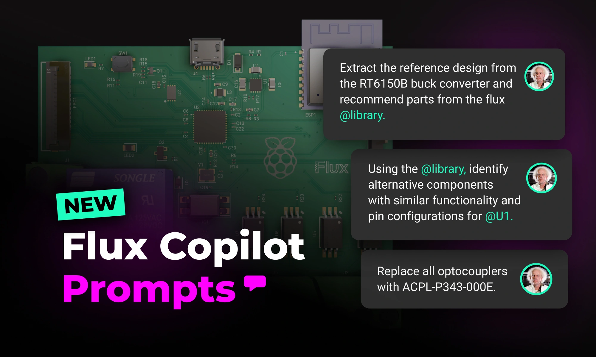
With the latest release of Copilot it isn’t just smarter—it’s hands-on, placing components and applying bulk changes to your project instantly. But to get the most out of it, knowing how to craft the right prompt is key.

Profile avatar of Ryan Fitzgerald
Ryan Fitzgerald
|March 13, 2025
Introducing the AI Design Review Tab

Introducing the AI Design Review Tab

Creating a manufacturable, error-free PCB is never simple. Every engineer knows that missed details lead to production delays, costly revisions, and project setbacks. But what if you could have the power of a seasoned review team guiding you, 24/7?

Profile avatar of Lance Cassidy
Lance Cassidy
|November 7, 2024
EasyEDA vs. Flux

EasyEDA vs. Flux

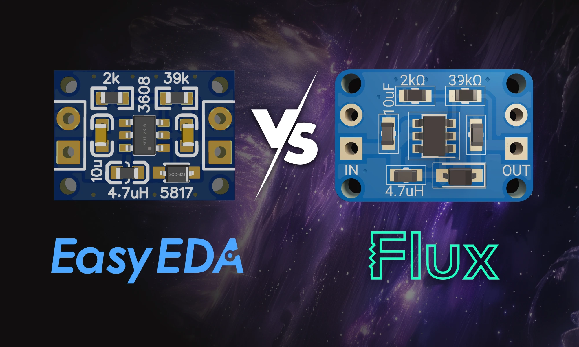
If you’re using EasyEDA and are thinking of making the switch to Flux, learn how the two platforms differ and why Flux might be the next step in elevating your PCB design experience.

Profile avatar of Ryan Fitzgerald
Ryan Fitzgerald
|October 17, 2024
5 Common Mistakes Working with PCB Contractors

5 Common Mistakes Working with PCB Contractors

In this post, we’ll explore five common mistakes companies make when contracting PCB design and how you can avoid them by using tools like Flux to keep your project on track, from concept to completion.

Profile avatar of Nico Tzovanis
Nico Tzovanis
|October 10, 2024