May 8, 2025
Smart Polygons: Advanced PCB Design Just Got Easier
Share

Smart Polygons in Flux behave intuitively like traces, making them straightforward to learn and use—start directly from any pad with automatic net association, simply click to place and adjust points, and watch as copper intelligently reflows in real-time. Let’s dive in!
In PCB design, polygons are customizable copper shapes directly tied to a specific net. They’re crucial because they significantly influence the electrical performance and reliability of your PCB. Polygons allow you to optimize your board layout for specific electrical properties, including improved grounding, controlled impedance, and efficient heat distribution.
Specifically, polygons are indispensable for:
Unlike zones—which define areas where copper cannot exist—polygons actively conduct electricity and shape your board's electrical performance, making them fundamental for advanced PCB designs.
At Flux, we prioritize intuitive, user-friendly workflows. Automatic copper fills were the first step. Now with polygons, we've continued this approach:

Polygons in Flux behave intuitively like traces, making them straightforward to learn and use, right from the start.
Polygons in Flux pack powerful functionality without complexity:

Polygons unlock new possibilities in your PCB designs. Here are a few practical ways you'll benefit:


Whether you're just dipping your toes into PCB design or you’re a veteran engineer tackling complex layouts, polygons in Flux offer the ideal balance of simplicity and capability:
Polygons are available now in Flux, ready to enhance your PCB design capabilities. Explore this powerful feature today and experience firsthand how advanced design can truly be this easy.
Dive in now and check out our detailed polygon documentation or jump straight into Flux to try it yourself. We can't wait to hear what you think!


With the latest release of Copilot it isn’t just smarter—it’s hands-on, placing components and applying bulk changes to your project instantly. But to get the most out of it, knowing how to craft the right prompt is key.
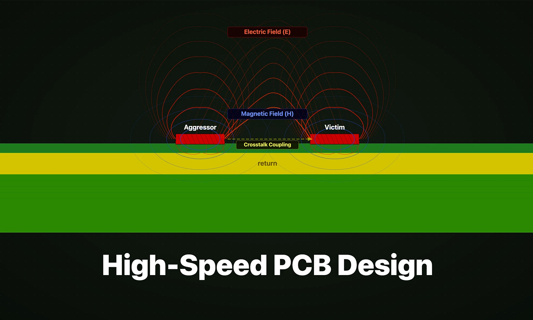
Whether you're migrating from popular EDA applications or starting fresh, mastering high speed PCB design has never been more intuitive. Flux enables teams to design, simulate, and route with real-time AI assistance, so you can spin your next high-speed board with total confidence.

Now, Flux Copilot can learn how you work—your design principles, part selection preferences, schematic style guidelines, and testing workflows—and remember them automatically.

Imagine an AI teammate that doesn’t just chat about your PCB ideas, but actively transforms them into schematics—placing parts, connecting circuits, and optimizing your design at your command, all through natural language. That’s exactly what the newly overhauled Flux Copilot does.

Creating a manufacturable, error-free PCB is never simple. Every engineer knows that missed details lead to production delays, costly revisions, and project setbacks. But what if you could have the power of a seasoned review team guiding you, 24/7?

If you’re using EasyEDA and are thinking of making the switch to Flux, learn how the two platforms differ and why Flux might be the next step in elevating your PCB design experience.

KiCad revolutionized PCB design by making it accessible to everyone. Flux builds on that foundation, offering a browser-based, AI-powered platform that takes your PCB design experience to the next level.

Flux's upgraded agent is more steerable, adaptive, and faster -- letting you change course mid-run, work in a single thread from idea to board, and ship hardware designs with less friction.
