June 5, 2026
Schematic Capture Explained: How Engineers Create Circuit Diagrams
Share

Every piece of modern hardware, from a simple blinking LED badge to the motherboard of a supercomputer, begins as an idea. However, before that idea can be manufactured as a physical Printed Circuit Board (PCB), it must be translated into a formal, machine-readable language. This foundational translation process is known as schematic capture.
For engineers, students, and hardware designers, understanding schematic capture is the first step in the electronic design journey. It is the process where electrical theory meets practical engineering software. This guide breaks down what schematic capture is, the core elements involved, and how modern tools are transforming the way teams create circuit diagrams.
Schematic capture (or schematic entry) is the process of using Electronic Design Automation (EDA) software to create a logical representation of an electronic circuit.
During this phase, engineers do not worry about the physical size of the board, the length of the copper traces, or where the mounting holes will go. Instead, electronic schematic capture focuses entirely on electrical intent: which components are used, what their values are, and exactly how their pins connect to one another to achieve the desired functionality. The lines in a schematic represent connectivity between components (nets), not the actual length or physical routing of wires on the PCB.
The final output is a schematic diagram, a 2D blueprint that serves as both the operational roadmap for the circuit and the official documentation for the engineering team.
It is impossible to design a complex, functional circuit board without first performing schematic capture. The schematic acts as the brains of the operation, driving several downstream processes in PCB manufacturing:
To perform schematic capture effectively, engineers use a standardized set of visual building blocks.
| Element | Description | Engineering Best Practice |
|---|---|---|
| Symbols | Graphical representations of electronic components (resistors, ICs, diodes). They abstract physical parts into simple, readable shapes. | Always use verified symbols from trusted libraries to ensure the pins map correctly to the physical footprint. |
| Nets (Wires) | The lines drawn between component pins that represent electrical connections. | Label important nets (e.g., "I2C_SCL" or "5V_MAIN"). Named nets help trace signals across complex, multi-page designs. |
| Junctions | Solid dots placed where two crossing nets intersect, indicating that they are electrically tied together. | If two nets cross without a dot, they do not connect. Missing or accidental junctions are major sources of circuit failure. |
| Power & Ground Ports | Specialized symbols indicating connections to power rails (VCC, 3.3V, 5V) and ground (GND) references. | Use ports instead of drawing long, messy nets across the entire page back to a single battery symbol. This keeps the diagram clean. |
The workflow within modern circuit schematic software generally follows a standardized, step-by-step process.
For beginners learning circuit diagram creation, avoiding these common pitfalls will save hours of debugging later:
Historically, schematic capture was an isolated, desktop-bound process. Engineers would draw the schematic, export a static netlist, and pass it to the PCB layout designer. Any design change required repeating the export/import process, often creating version-control issues.
Modern platforms like Flux are redefining this workflow with collaborative, browser-based schematic editors. In Flux, the schematic editor allows engineers to build, simulate, and edit circuits with real-time cloud synchronization. The interface includes integrated chat, component libraries, and contextual inspectors for properties, pricing, and design data.
Unlike traditional tools, the schematic and PCB layout remain dynamically linked. When a component is added or modified in the schematic, the PCB layout updates instantly, eliminating manual netlist exports. Because the platform is multiplayer, engineers and PCB designers can collaborate on the same project simultaneously.
Flux also integrates an AI-powered hardware design assistant directly into the schematic editor. The AI understands the full project context, including schematics, components, electrical connections, BOM data, and datasheets. This enables features such as part selection, alternate component evaluation, design feedback, cost optimization, and circuit design assistance, transforming schematic capture from a drafting task into a faster, more intelligent engineering workflow. Try Flux now to start designing circuits faster with real-time collaboration and AI-assisted schematic capture.


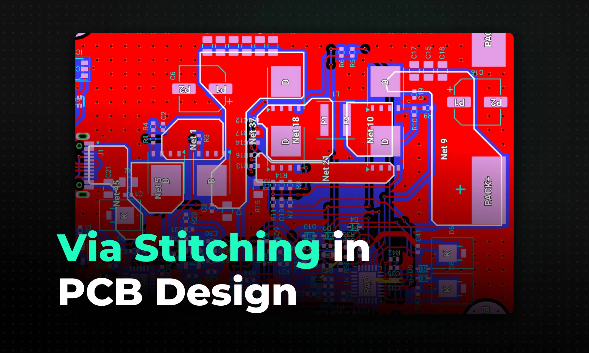
A practical guide to via stitching in PCB design -- what it is, why it improves EMI, signal integrity, and thermal performance, and where to place stitching vias. Includes spacing rules (like lambda/20), design guidelines, common mistakes to avoid, and how Flux can automate stitching via placement.
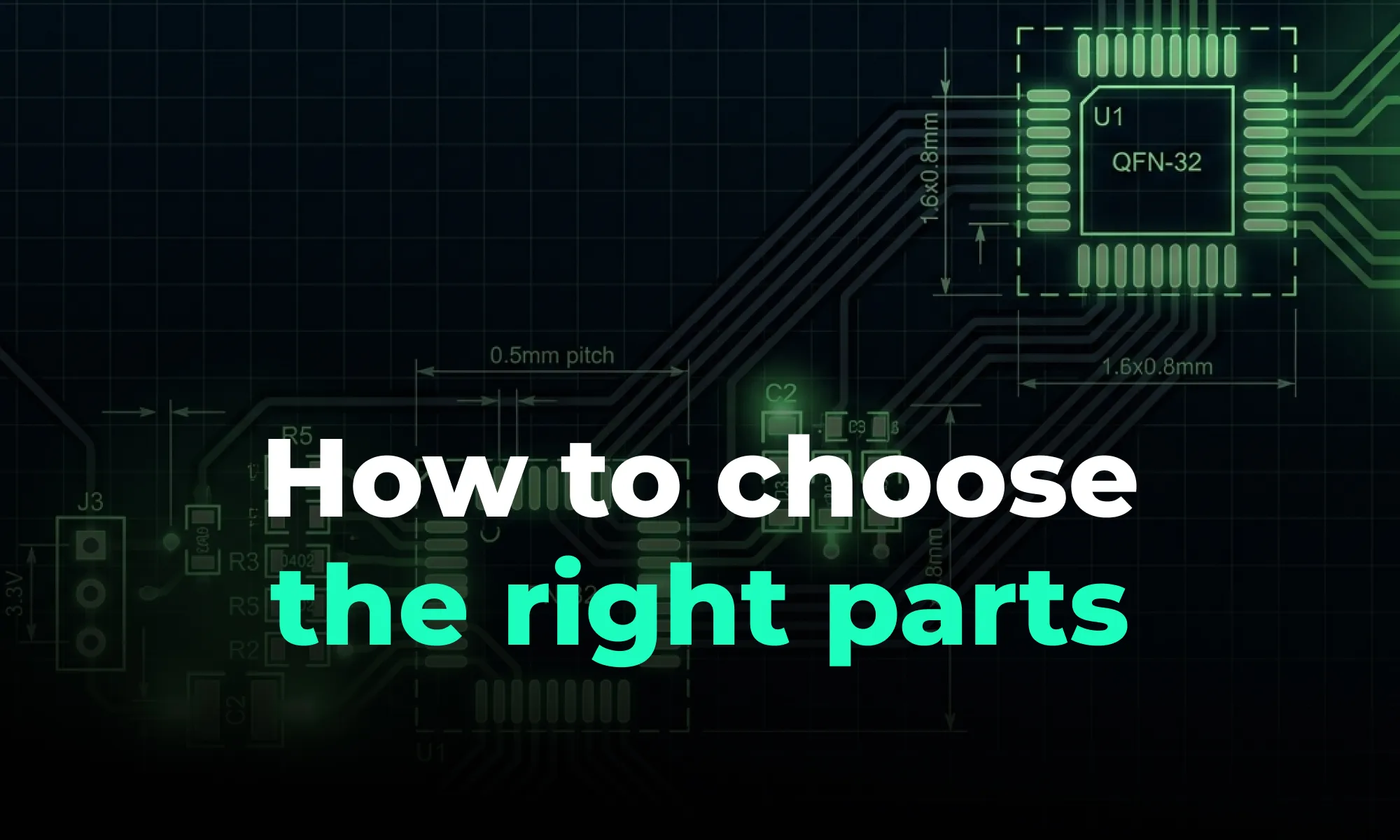
A guide to PCB component selection, covering electrical specs, footprints, thermal performance, sourcing, and best practices for picking parts that ship reliably.

A guide to PCB design reviews, covering schematic, layout, and DFM checks engineers use to catch errors early and ship more reliable boards.

A guide to creating and managing PCB footprint libraries, covering IPC standards, pad sizing, validation workflows, and best practices for reliable land patterns.

A guide to PCB schematic best practices, covering organization, symbols, labeling, and readability tips for clean, maintainable circuit diagrams.

A guide to flexible PCB design, covering materials, stackups, bend radius, and layout best practices for wearables, medical devices, and other compact electronics.

A beginner-friendly guide to reading PCB schematics, covering common symbols, nets, and how to follow signal flow through a circuit diagram.

An overview of collaborative PCB design, showing how cloud-native tools, real-time editing, and shared libraries are reshaping modern hardware team workflows.
