April 24, 2026
PCB Stackup Design: How to Build the Right Layer Structure
Share

As signal speeds increase and components shrink, the way designers arrange copper and insulating layers in a PCB stackup becomes a deciding factor in whether a design succeeds or fails.
Intelligent PCB stackup design allows engineers to manage noise, ensure stable power delivery, and maintain signal integrity. This guide breaks down the fundamentals of building a PCB stackup structure that meets both electrical requirements and manufacturing constraints.
PCB stackup design is the arrangement of conductive copper layers and insulating dielectric materials that make up a multilayer circuit board. The PCB stackup defines the thickness of each layer, the material for each layer and subsequent properties (such as dielectric constant, or Dk), and the specific function assigned to each copper layer.
A typical stackup consists of three main elements:
By carefully planning this structure, designers can create a controlled environment for signal propagation, rather than just a series of random connections.
A poorly planned stackup results in "black magic" issues, intermittent errors that are difficult to debug. A strategic design addresses three core areas:
Understanding the PCB layer configuration requires assigning specific roles to each copper layer.
Between and around these copper layers are dielectric materials, which include both core and prepreg:
Both core and prepreg are dielectric (insulating) layers, and together they define the electrical spacing between copper layers, which directly affects impedance, signal integrity, and propagation speed.
Designing a stackup is an iterative process that must be finalized before routing begins.
| Layer Count | Typical Structure | Best Used For |
|---|---|---|
| 2 Layers | Top (Signal), Bottom (Signal/GND) | Simple, low-speed analog or power circuits. |
| 4 Layers | Signal, GND, PWR, Signal | Standard microcontrollers and low-speed digital. |
| 6 Layers | Signal, GND, Signal, Signal, PWR, GND | High-speed designs needing better EMI shielding. |
| 8 Layers | Signal, GND, Signal, GND, PWR, Signal, GND, Signal | Complex designs, high-pin-count BGAs, and RF. |
In a controlled impedance PCB, the trace width is calculated based on the distance to the nearest continuous reference plane and the dielectric constant (Dk) of the material. If the manufacturer uses a different prepreg thickness than you planned, your 50Ω traces might actually be 60Ω, causing reflections that break high-speed communication.
Further, maintaining symmetry in layer thickness and copper distribution is critical, an unbalanced stackup can warp during lamination, leading to manufacturing defects and inconsistent electrical performance.
Always consult your fabrication house early. Most manufacturers provide "standard" stackups that are already verified for common impedance targets. Using these pre-built structures reduces cost and improves production yield.
Traditional design tools often treat the stackup as a secondary table or a separate spreadsheet. This disconnect makes it easy to lose track of how a change in layer thickness impacts the traces you've already routed.
Modern platforms like Flux bring the stackup into a visual, real-time environment. By integrating the layer structure directly with the layout, engineers can see the immediate impact of material choices on impedance and clearance. Collaborative features allow you to share your PCB stackup design with team members or manufacturers for instant feedback, ensuring the board is buildable long before you hit the "order" button.


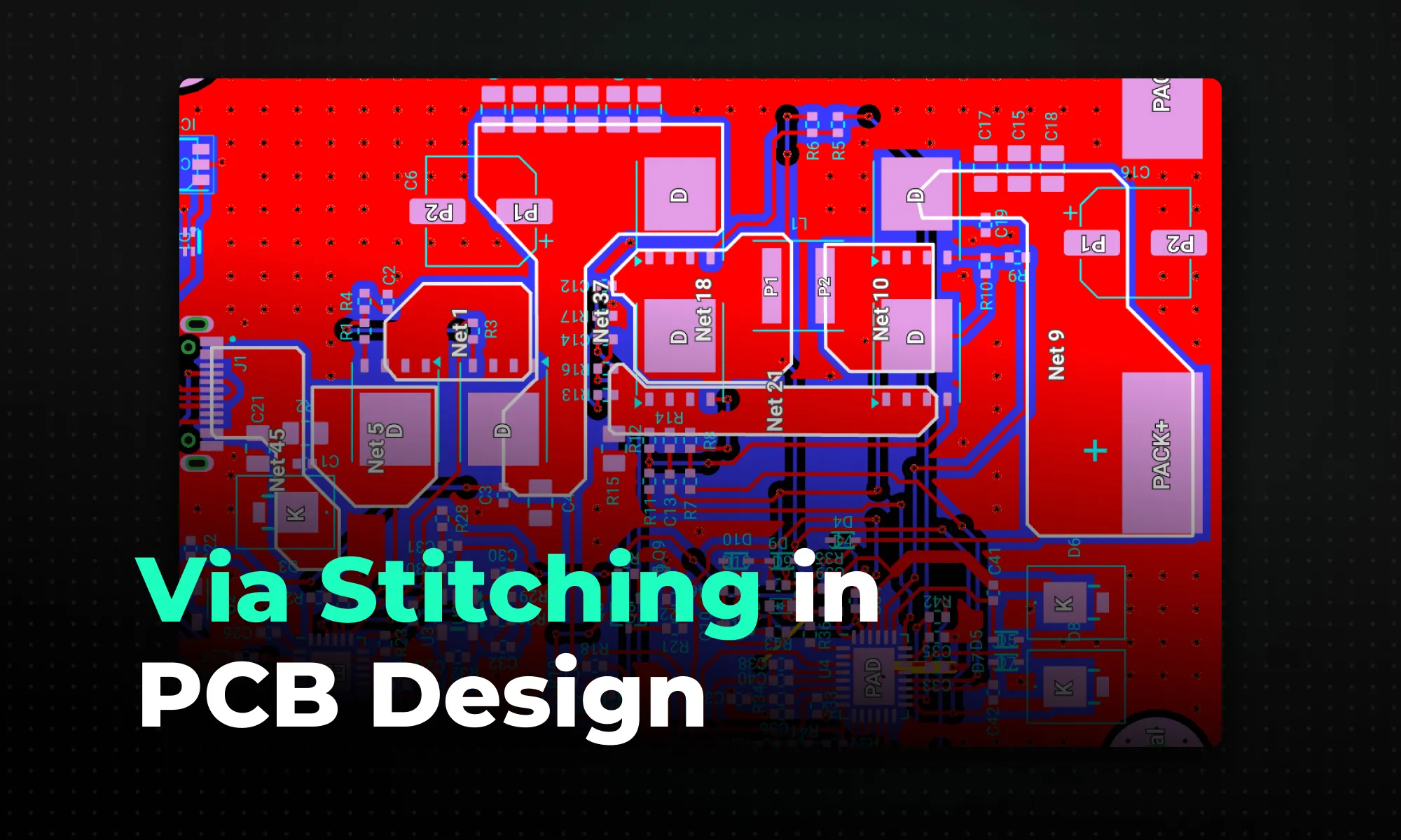
A practical guide to via stitching in PCB design -- what it is, why it improves EMI, signal integrity, and thermal performance, and where to place stitching vias. Includes spacing rules (like lambda/20), design guidelines, common mistakes to avoid, and how Flux can automate stitching via placement.

A guide to PCB component selection, covering electrical specs, footprints, thermal performance, sourcing, and best practices for picking parts that ship reliably.

A guide to PCB design reviews, covering schematic, layout, and DFM checks engineers use to catch errors early and ship more reliable boards.

A guide to creating and managing PCB footprint libraries, covering IPC standards, pad sizing, validation workflows, and best practices for reliable land patterns.

A guide to PCB schematic best practices, covering organization, symbols, labeling, and readability tips for clean, maintainable circuit diagrams.

A guide to flexible PCB design, covering materials, stackups, bend radius, and layout best practices for wearables, medical devices, and other compact electronics.

A beginner-friendly guide to reading PCB schematics, covering common symbols, nets, and how to follow signal flow through a circuit diagram.

An overview of collaborative PCB design, showing how cloud-native tools, real-time editing, and shared libraries are reshaping modern hardware team workflows.
