April 27, 2026
PCB Impedance Control: A Practical Guide for Engineers
Share

At high speeds, a PCB trace is not a wire. Once signal frequencies climb past 100 MHz or edge rates get fast enough, traces start behaving as transmission lines, and the rules of signal propagation change entirely. Fail to control impedance, and you will deal with reflections, data corruption, and timing failures that are notoriously difficult to debug on a finished board.
In DC circuits, resistance opposes current flow. In high-frequency circuits, traces exhibit characteristic impedance -- a property that determines how electromagnetic energy propagates along the trace. Unlike resistance, impedance is not about energy loss; it is about energy transfer.
When an electrical signal travels down a trace, it creates both an electric field (between the trace and the reference plane) and a magnetic field (around the trace). Characteristic impedance is the ratio of voltage to current of this traveling wave. For a uniform trace over a uniform reference plane, this ratio is constant along the entire length.
In practice, most high-speed interfaces are designed around a characteristic impedance of for single-ended signals and for differential pairs (USB, Ethernet, PCIe). These are not arbitrary values; they represent historical engineering compromises between signal loss, power handling, and ease of manufacturing.
When a signal hits a point where the impedance changes abruptly -- a connector, a via, or a trace width change -- part of the energy reflects back toward the source. This reflected energy interferes with the next incoming bit, creating waveform distortion.
For a high-speed bus like DDR4 running at 3200 MT/s, the data eye is roughly 300 picoseconds wide. A reflection that arrives even 50 ps late can close the eye, causing bit errors. As signal integrity requirements tighten, even small deviations from target impedance cause measurable degradation.
The severity of a reflection at any impedance discontinuity is governed by the reflection coefficient:
Where is the impedance before the discontinuity and is the impedance after. If , is zero and no energy reflects. A 10% impedance mismatch produces approximately a 5% reflection, which may be tolerable for slower signals but is destructive at GHz frequencies.
Characteristic impedance of a microstrip or stripline is determined by four physical parameters. All are set during stackup design and fabrication, which is why impedance planning must happen before routing starts.
A wider trace stores more capacitance per unit length relative to its reference plane, which reduces impedance. Narrowing the trace increases impedance. This is the primary adjustment mechanism available to the designer during layout.
The distance between the trace and its reference plane -- determined by the prepreg or core thickness in the stackup -- directly affects the electric field coupling. A smaller gap increases capacitance and lowers impedance; a larger gap does the opposite.
Thicker copper slightly increases the effective width of the trace due to edge effects (known as "etch factor"), which marginally reduces impedance. In most cases, copper thickness has a smaller impact than width or height, but it must still be included in calculations for accuracy.
The dielectric constant of the insulating material between the trace and the reference plane determines how much capacitance the geometry creates. Standard FR-4 has a Dk of roughly 4.2-4.5. Low-loss materials used for high-speed designs (such as Megtron 6 or Rogers laminates) have different Dk values. Critically, Dk varies with frequency, so the value used in calculations must correspond to the signal's operating frequency.
The two fundamental trace structures in a PCB are microstrip and stripline:
The impedance formulas are different for each structure. No single equation covers all cases, and most practical design relies on 2D field solver software built into modern PCB tools.
Achieving controlled impedance is not a single step. It is an end-to-end discipline that spans from schematic intent through fabrication.
Identify which nets require controlled impedance from the component datasheets and interface specifications. USB 2.0 specifies differential impedance. PCIe Gen 4 specifies differential. SPI, I2C, and other low-speed buses generally do not require impedance control.
Work with your fabricator to define layer thicknesses and materials that achieve your target impedance for a practical trace width. A good stackup should allow you to hit single-ended with a trace width between 4-6 mils on outer layers. If the required width is impractically narrow or wide, adjust the dielectric thickness or material.
Assign impedance-controlled net classes in your EDA tool. These net classes enforce the calculated trace widths and spacing rules during routing. Any violation should trigger a DRC error.
Provide an impedance control table in your fabrication notes specifying the target impedance, tolerance (typically +/- 10%), the layers involved, and the reference planes. The fabricator will use a TDR (Time Domain Reflectometer) to verify impedance on test coupons included in the production panel.
Traditional EDA workflows require constant manual cross-referencing between stackup spreadsheets, impedance calculators, and routing constraints. Flux eliminates this fragmentation.
Flux's integrated stackup editor ties material properties directly to the layout. When you define a stackup with specific dielectric thicknesses and Dk values, the platform dynamically calculates the required trace widths for your impedance targets. If you change a prepreg thickness, the impedance constraints update automatically -- no manual recalculation needed.
The AI-powered design review system can flag impedance discontinuities, trace width violations, and reference plane gaps during layout, catching the kind of errors that traditionally surface only during post-layout simulation or, worse, during board bring-up.


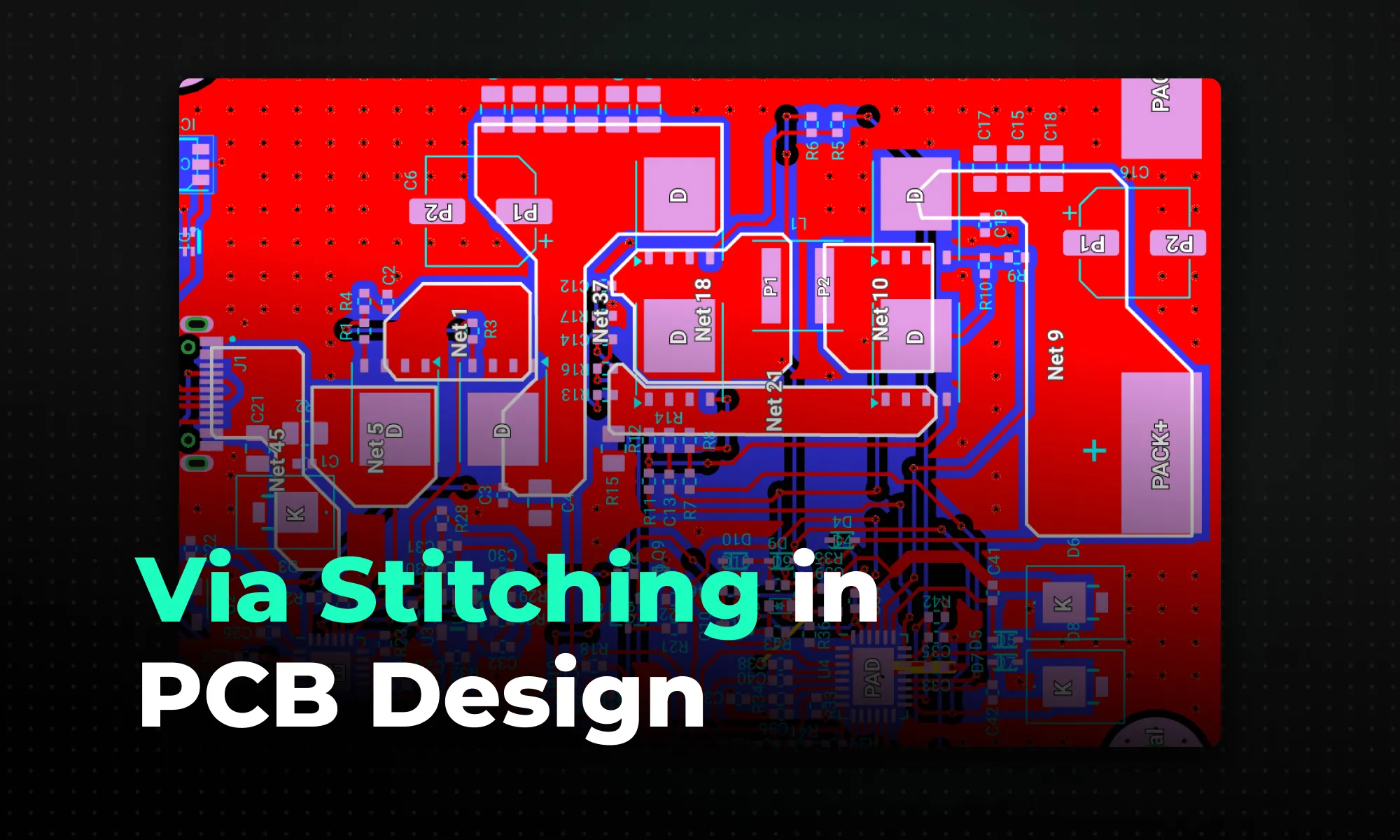
A practical guide to via stitching in PCB design -- what it is, why it improves EMI, signal integrity, and thermal performance, and where to place stitching vias. Includes spacing rules (like lambda/20), design guidelines, common mistakes to avoid, and how Flux can automate stitching via placement.

A guide to PCB component selection, covering electrical specs, footprints, thermal performance, sourcing, and best practices for picking parts that ship reliably.

A guide to PCB design reviews, covering schematic, layout, and DFM checks engineers use to catch errors early and ship more reliable boards.

A guide to creating and managing PCB footprint libraries, covering IPC standards, pad sizing, validation workflows, and best practices for reliable land patterns.

A guide to PCB schematic best practices, covering organization, symbols, labeling, and readability tips for clean, maintainable circuit diagrams.

A guide to flexible PCB design, covering materials, stackups, bend radius, and layout best practices for wearables, medical devices, and other compact electronics.

A beginner-friendly guide to reading PCB schematics, covering common symbols, nets, and how to follow signal flow through a circuit diagram.

An overview of collaborative PCB design, showing how cloud-native tools, real-time editing, and shared libraries are reshaping modern hardware team workflows.
