September 12, 2024
High-Density PCBs just got easier with Smart Vias
Share

Even for the most experienced engineers, high density interconnect designs remain difficult. Some typical challenges are:
Traditional EDA tools depend heavily on manual input for via placement. This makes density management primarily a function of hand-eye coordination. After placement, when you need to modify part of the design, you’ll quickly find yourself playing an unsolicited game of three-dimensional chess. Often, it’s easiest to simply wipe out the traces and vias, start over, and hope you won’t have to make another change to that part of your board.
After carefully laying everything out, the next big effort is to define and work through manufacturability, reliability, and cost considerations. In practice, this mountain of manual labor adds up. Designers are often forced to either compromise their design, risk overlooking mistakes, or delay their project.
Smart Vias in Flux is an intelligent feature that automates the selection, placement, and configuration of vias during the PCB design process. This automation reduces the manual effort involved in via placement and significantly lowers the risk of misalignment and other common errors associated with traditional via management
If you’re routing a trace and need to connect across multiple layers, Flux will place a Smart Via that automatically populates with the best suited combination of vias (micro, blind, buried, or through-hole), in a stacked or staggered configuration, respecting your project settings. For example, you might only want to use microvias on outer layers and use through-hole vias for everything else. With Smart Vias, you can just start routing. When you switch from Top to Mid-Layer 1, a Smart Via will get you there. You can change your mind and go to Bottom and the Smart Via will dynamically reconfigure itself to support that connectivity.

Smart Vias are powered by Flux’s innovative Layout Rules. Rules allow you to set your preferences from a central place in the Stackup. They also allow for control of individual Smart Vias right down to the details, like the direction or spacing of a stagger. The result is a feature gets out of your way when you want and also lets you sweat the small stuff.
To make it even easier to get started, simply clone or fork any of these templates.
Overall, Smart Vias addresses many of the challenges inherent in high density interconnect design and offers notable benefits to the designer.
We think this is a huge improvement over existing workflows and we’re excited for you to use it. Interested in experiencing the new Smart Via feature? Get started with a template today!


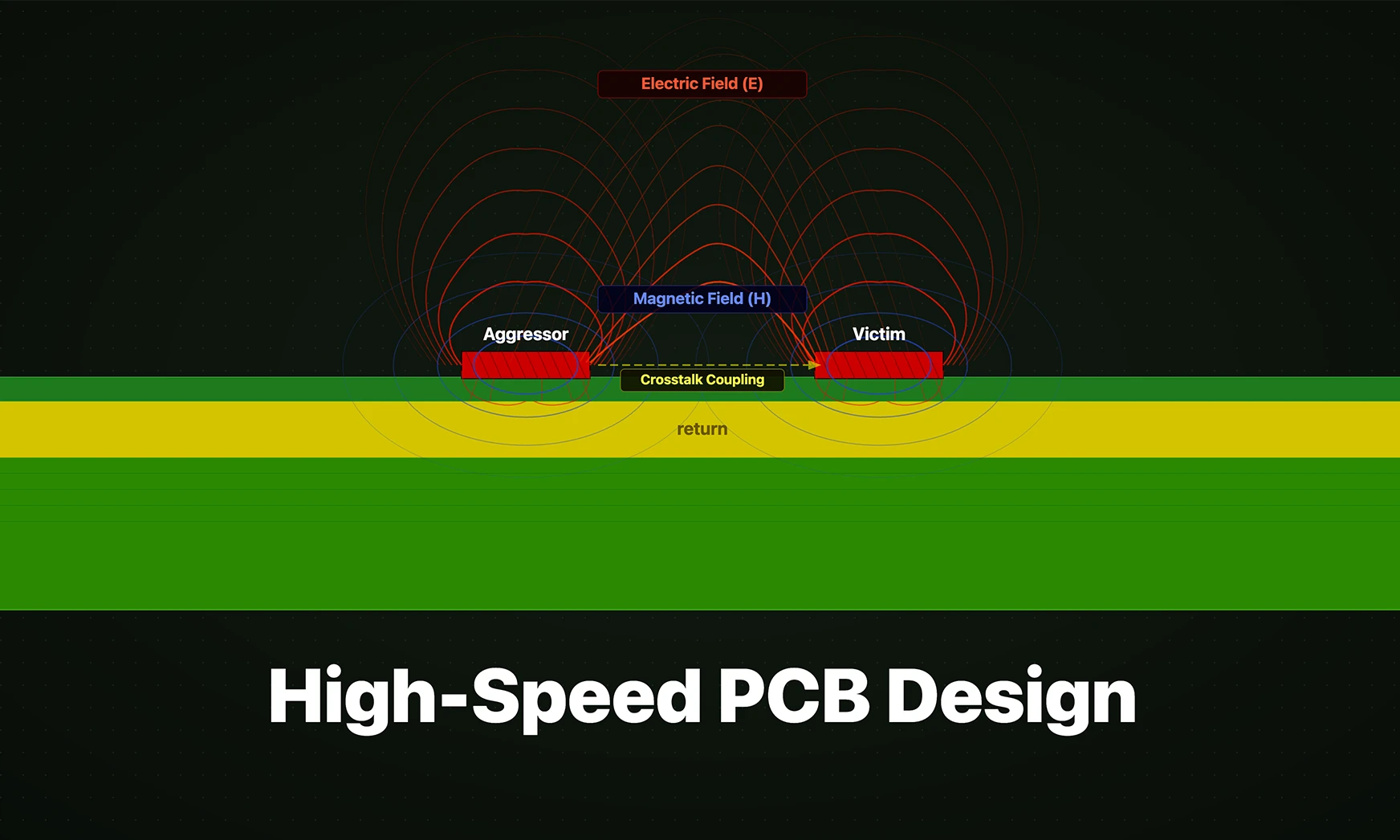
Whether you're migrating from popular EDA applications or starting fresh, mastering high speed PCB design has never been more intuitive. Flux enables teams to design, simulate, and route with real-time AI assistance, so you can spin your next high-speed board with total confidence.
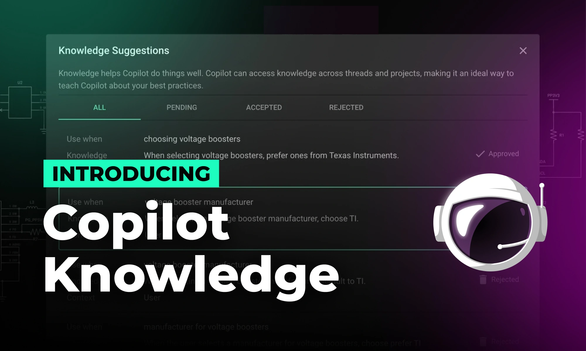
Now, Flux Copilot can learn how you work—your design principles, part selection preferences, schematic style guidelines, and testing workflows—and remember them automatically.

We're excited to unveil our Smart Polygon system in Flux! This powerful capability builds on top of our automatic copper fills to transform how you create and manage custom copper areas in your PCB designs.

With the latest release of Copilot it isn’t just smarter—it’s hands-on, placing components and applying bulk changes to your project instantly. But to get the most out of it, knowing how to craft the right prompt is key.

Creating a manufacturable, error-free PCB is never simple. Every engineer knows that missed details lead to production delays, costly revisions, and project setbacks. But what if you could have the power of a seasoned review team guiding you, 24/7?

If you’re using EasyEDA and are thinking of making the switch to Flux, learn how the two platforms differ and why Flux might be the next step in elevating your PCB design experience.

KiCad revolutionized PCB design by making it accessible to everyone. Flux builds on that foundation, offering a browser-based, AI-powered platform that takes your PCB design experience to the next level.

Discover our latest schematic design updates that streamline wire adjustments, component alignment, and intuitive pin connections, making your design process faster and meeting your high standards for precision. These enhancements, coupled with our AI design assistant, ensure a solid foundation for your projects.
