Switches
A switch is a device that allows electricity to flow through a circuit by completing or interrupting the connection. It is a common component in electrical and electronic systems and is used in a variety of applications, such as controlling the flow of electricity in a circuit, turning devices on and off, and routing electrical signals. One of the primary use cases for switches is to control the flow of electricity in a circuit. This can be done by manually flipping the switch or by using a control mechanism, such as a timer or a sensor. Another common use for switches is to turn devices on and off. This can be done using a switch that is built into the device or by using a separate switch that is connected to the device. In addition to these basic use cases, switches can also be used to route electrical signals. For example, a switch can be used to route a signal from one device to another or to direct a signal to a specific circuit or component. If you're looking for a wide variety of switches for your projects, flux.ai has the world's largest community-driven public library of them. The library includes footprints, symbols, datasheets, and simulation models for a wide range of switches, making it easy to find the right switch for your needs.
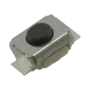
TS-1088-AR02016
50mA 4mm 100MΩ 100,000 Times 12V 160gf 3mm 2mm Round Button Vertical welding SPST SMD Tactile Switches ROHS Tactile Switches TS-1088-AR02016 SW-SMD_L3.9-W3.0-P4.45 LCSC Part Number: C720477 JLCPCB Part Class: Extended Part Manufactured by XUNPU(讯普) momentary tactile switch, SMD 6 mm tactile push button, through-hole SPST on/off mechanical switch momentary pushbutton for BOOT / RESET / PTT
5.3k Uses1 StarsADS8688IDBTR
16 Bit Analog to Digital Converter 8 Input 1 SAR 38-TSSOP The ADS8688IDBTR specification defines the engineering requirements for a multi-channel analog-to-digital converter integrated circuit designed for precision data acquisition and signal measurement applications. This specification establishes the functional, electrical, mechanical, thermal, environmental, and quality requirements necessary to ensure accurate analog signal conversion, reliable digital communication, and long-term operational stability in embedded and industrial electronic systems. The device is intended for use in industrial automation, process control, instrumentation, medical equipment, test and measurement systems, energy monitoring, and embedded control applications requiring simultaneous access to multiple analog input channels. The integrated analog front end and high-resolution conversion architecture provide accurate signal acquisition while simplifying system design and reducing external component requirements. Engineering Requirements The analog-to-digital converter shall be manufactured using qualified semiconductor fabrication processes and high-quality materials to ensure consistent conversion accuracy, low noise performance, and dependable long-term reliability. The device shall maintain stable operation under specified voltage, temperature, and environmental operating conditions. Electrical characteristics shall provide high-resolution analog-to-digital conversion, excellent linearity, low offset error, and stable reference performance. The converter shall support reliable multi-channel signal acquisition while maintaining low distortion, repeatable sampling accuracy, and consistent digital output throughout continuous operation. The integrated acquisition architecture shall provide reliable channel selection, input signal conditioning, and high-speed serial communication with compatible host processors. The device shall maintain signal integrity during channel switching, startup, shutdown, and dynamic operating conditions while minimizing conversion errors and communication latency. Thermal performance shall support continuous operation within the specified junction temperature range while maintaining electrical characteristics and long-term reliability. The package shall be suitable for automated surface-mount assembly and compatible with standard solder reflow manufacturing processes. Mechanical construction shall withstand thermal cycling, vibration, mechanical handling, and environmental exposure without degradation of electrical or mechanical performance. Workmanship shall be free from defects including contamination, package cracking, bond failures, lead deformation, or structural inconsistencies that could adversely affect device functionality or reliability. Inspection, validation, and testing shall be performed using calibrated equipment and controlled quality procedures to verify compliance with engineering and manufacturing requirements. Any deviation from this specification shall require formal engineering evaluation, documented technical justification, and approval through the established engineering change control process before implementation. Documentation Supporting documentation shall include engineering drawings, electrical performance specifications, timing diagrams, application guidelines, qualification reports, inspection records, reliability data, material declarations, and revision-controlled manufacturing documentation. All documentation shall be maintained under formal configuration management and quality assurance systems to ensure complete product traceability. Revision Control Any modification to this specification shall be managed through the formal engineering change management process. All revisions shall undergo technical review, validation, and approval before release to ensure continued compliance with design intent and applicable engineering standards. #EngineeringSpecification #AnalogToDigitalConverter #ADC #DataAcquisition #SignalConditioning #IndustrialAutomation #EmbeddedSystems #Instrumentation #QualityAssurance #EngineeringDocumentation
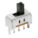
21 Uses1 StarsOS102011MS2QN1
Slide Switch, SPDT, On-On, Through Hole, OS Series, 100mA # OS102011MS2QN1 ## General Description The OS102011MS2QN1 is a miniature slide switch manufactured by C&K, designed for low-power signal switching and control applications in electronic equipment. The switch features a compact mechanical design, reliable contact performance, and through-hole mounting configuration, making it suitable for embedded systems, industrial controls, instrumentation, telecommunications equipment, consumer electronics, and portable devices. Its robust construction ensures dependable operation throughout repeated switching cycles while maintaining stable electrical performance. The device is commonly utilized for mode selection, power control, configuration settings, and user-interface functions within electronic assemblies. ## Key Features ### Mechanical Characteristics * Miniature slide switch construction * Through-hole PCB mounting * Compact form factor * Durable actuator mechanism * Positive switching action * Designed for repeated mechanical operation ### Switching Characteristics * Maintained-contact operation * Reliable position retention * Low-force actuation * Stable contact engagement * Suitable for signal and control switching applications ### Electrical Characteristics * Low contact resistance * Reliable signal transmission * Stable switching performance * Suitable for low-current and low-voltage circuits * Consistent electrical operation throughout service life ### Contact System * High-reliability contact materials * Corrosion-resistant contact surfaces * Long operational durability * Dependable electrical continuity ### Material Construction * High-strength thermoplastic housing * Industrial-grade metallic contacts * Durable actuator assembly * RoHS-compliant materials ### Environmental Characteristics * Suitable for commercial and industrial electronic equipment * Resistant to mechanical wear * Reliable performance under normal operating environments * Designed for long-term service reliability ### Application Areas * Embedded Systems * Industrial Control Equipment * Consumer Electronics * Test and Measurement Instruments * Communication Devices * Medical Electronics * Power Control Circuits * User Interface Controls * Configuration and Mode Selection Functions * Electronic Development Platforms ### Compliance * RoHS Compliant * Lead-Free Compatible * Industrial-Grade Switching Component ## Manufacturer C&K ## Product Family OS Series Miniature Slide Switches #OS102011MS2QN1 #CKSwitches #SlideSwitch #MiniatureSwitch #ElectronicSwitch #PCBSwitch #EmbeddedSystems #IndustrialElectronics #ControlSystems #ConsumerElectronics #HardwareDesign #ElectronicsEngineering #SignalSwitching #PCBAssembly #ElectronicComponents #commonpartslibrary #switch #slide #spdt
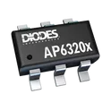
670 Uses1 StarsAP63203WU-7
Buck Switching Regulator IC Positive Fixed 3.3V 1 Output 2A SOT-23-6 Thin, TSOT-23-6 The AP63200/AP63201/AP63203/AP63205 is a 2A, synchronous buck converter with a wide input voltage range of 3.8V to 32V and fully integrates a 125mΩ high-side power MOSFET and a 68mΩ low-side power MOSFET to provide high-efficiency step-down DC/DC conversion. The AP63200/AP63201/AP63203/AP63205 device is easily used by minimizing the external component count due to its adoption of peak current mode control along with its integrated compensation network. The AP63200/AP63201/AP63203/AP63205 has optimized designs for Electromagnetic Interference (EMI) reduction. The converter features Frequency Spread Spectrum (FSS) with a switching frequency jitter of ±6%, which reduces EMI by not allowing emitted energy to stay in any one frequency for a significant period of time. It also has a proprietary gate driver scheme to resist switching node ringing without sacrificing MOSFET turn-on and turn-off times, which further erases highfrequency radiated EMI noise caused by MOSFET switching. The device is available in a low-profile, TSOT26 package. • VIN 3.8V to 32V • 2A Continuous Output Current • 0.8V ±1% Reference Voltage • 22µA Ultralow Quiescent Current • Switching Frequency o 500kHz: AP63200 and AP63201 o 1.1MHz: AP63203 and AP63205 • Pulse Width Modulation (PWM) Regardless of Output Load o AP63201 • Supports Pulse Frequency Modulation (PFM) o AP63200, AP63203, and AP63205 o Up to 80% Efficiency at 1mA Light Load o Up to 88% Efficiency at 5mA Light Load • Fixed Output Voltage o 3.3V: AP63203 o 5.0V: AP63205 • Proprietary Gate Driver Design for Best EMI Reduction • Frequency Spread Spectrum (FSS) to Reduce EMI • Precision Enable Threshold to Adjust UVLO • Protection Circuitry o Overvoltage Protection o Cycle-by-Cycle Peak Current Limit o Thermal Shutdown • 12V and 24V distributed power bus supplies • Flat screen TV sets and monitors • Power tools and laser printers • White goods and small home appliances • FPGA, DSP, and ASIC supplies • Home audios • Network systems • Set top boxes • Gaming consoles • Consumer electronics #commonpartslibrary #integratedcircuit #AP63203WU7 #BuckConverter #DCDCConverter #PowerManagement #VoltageRegulator #SynchronousBuck #EmbeddedSystems #IndustrialElectronics #PowerSupply #DiodesInc #3V3Power #ElectronicsDesign
1.6k Uses1 StarsTLV62569DBVR
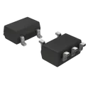
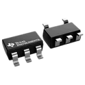
Buck Switching Regulator IC Positive Adjustable 0.6V Output 2A SC-74A, SOT-753 The Texas Instruments TLV62569DBVR is a high-efficiency synchronous step-down (buck) DC-DC converter designed for compact and low-power applications. It converts a higher DC input voltage down to a lower, regulated output voltage with high efficiency and small external component size. It is commonly used in portable electronics, embedded systems, routers, set-top boxes, and battery-powered devices where efficient power conversion and small footprint are important. 🔧 Key Features Input voltage range: 2.5 V to 5.5 V Output current capability: up to 2 A Adjustable output voltage: 0.6 V to VIN (via external resistors) High efficiency: up to ~95% Switching frequency: ~1.5 MHz (allows small inductors/capacitors) Synchronous rectification: improves efficiency by reducing losses Power Save Mode (PSM): boosts efficiency at light load Low quiescent current: ~35 µA typical 100% duty cycle support: low dropout operation 🛡️ Protection & Safety Features Overcurrent protection (OCP) Thermal shutdown protection Internal soft-start (reduces inrush current at startup) Power Good (PG) indicator for system monitoring 📦 Package SOT-23-5 (DBVR) Very small footprint for space-constrained PCB designs ⚙️ Typical Applications Point-of-load (POL) power supplies Wireless routers and networking devices Set-top boxes Battery-powered and portable systems Embedded controllers and IoT devices
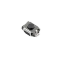
157 Uses1 StarsPTS810SJK250SMTRLFS
PTS 810 Series Microminiature SMT Top Actuated Features/Benefits - 4.2 x 3.2 mm footprint - 2.5 mm thickness - High number of cycles - Color coded actuators Typical Applications - Control panels - Nomad devices - Remote controls - Keyless entry system 3.2mm 2.5mm Round Button 50mA Brick nogging 4.2mm SPST 16V SMD Tactile Switch SPST-NO Top Actuated Surface Mount.
2.2k Uses1 Stars2N3904TFR
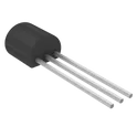
Bipolar (BJT) Transistor NPN 40V 200 mA 300MHz 625 mW Through Hole TO-92-3 The 2N3904TFR is a general-purpose NPN bipolar junction transistor (BJT) designed for low-power amplification and switching applications. It is widely used in signal processing, small-signal amplification, and digital switching circuits. This transistor offers fast switching speed, low saturation voltage, and reliable performance in a compact surface-mount package, making it suitable for consumer electronics, industrial controls, and embedded systems. Manufacturer Various (commonly ON Semiconductor / onsemi, Diodes Inc., Central Semiconductor) Part Number 2N3904TFR Transistor Type NPN Bipolar Junction Transistor (BJT) Configuration Single Package / Case SOT-23 (TO-236AB) Mounting Style Surface Mount (SMD/SMT) Collector-Emitter Voltage (VCEO) 40 V Collector-Base Voltage (VCBO) 60 V Emitter-Base Voltage (VEBO) 6 V Collector Current (IC) 200 mA (max) Power Dissipation (PD) ~200 mW to 350 mW (package dependent) DC Current Gain (hFE) 100 to 300 (typical, varies with operating conditions) Transition Frequency (fT) ~300 MHz Collector-Emitter Saturation Voltage (VCE(sat)) ~0.2 V (typical at IC = 10 mA, IB = 1 mA) Operating Temperature Range -55°C to +150°C Polarity NPN Packaging Tape & Reel (TFR suffix) RoHS Compliance Compliant #commonpartslibrary #transistor #bjt
920 Uses1 StarsHUSB238A-BB001-QN16R
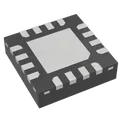
The HUSB238A is a highly integratedstand-aloneUSB Type-C® and Power Delivery (PD) Sinkcontroller.The HUSB238A integrates the CClogic, USBPDprotocol and the legacy protocols. The HUSB238A can run in I2C mode andGPIOmode.In I2C mode, an I2C master can access theHUSB238Ato configure settings, read back status andperformadvanced functions such as DRSwap, VDMmessages. The HUSB238A supports APDO, maximum48 V/5 A EPR FPDO and EPR AVSin I2Cmode. While in GPIO mode, the configuration is achievedviathe setting pins. The HUSB238A can beconfiguredtosupport maximum 28 V/3.25 A PDOviaVSETandISET pins, only two resistors are usedtoset thevoltage and current. The ultra-low operation current of theHUSB238Ahelps the system to reduce the total power dissipationand suitable for a battery application. The HUSB238A is available in QFN3 mmx3mm-16Lpackage. Fully Autonomous USB Type-C® and USB PD Sink Controller USB Type-C® Specification Reversion 2.1 and USB PD Specification Reversion 3.1 Supported Maximum 48 V/5 A PDO Supported – GPIO Mode: Maximum 28 V/3.25 A EPR FPDO and EPR AVS – I2C Mode: Maximum 48 V/5 A EPR FPDO, EPR AVS and SPR PPS Automatic Legacy Protocols Detection Including BC1.2, Divider 3, QC2.0 Support SOP’ Detection Typical Low Power Operation: IVDD< 75 μA Integrated VBUS Switch Driver Dead Battery Support VBUS Over-voltage Protection (OVP) and Under-voltage Protection (UVP) Over-temperature Protection (OTP) with Programmable Thresholds 2 kV HBM ESD Rating for USB IO Pins Small Package, 16 Lead QFN (3 mm x 3 mm) #CommonPartsLibrary #IntegratedCircuit #PowerManagement
166 Uses1 Stars