Resistors
A resistor is an electronic component that reduces the flow of current in a circuit. It is used to limit the amount of current flowing through a circuit, or to create a voltage drop in a circuit. One of the main uses of resistors is to protect components from too much current, which can cause damage or failure. Flux.ai is the world's largest community-driven public library of resistors, with footprints, symbols, datasheets, and simulation models. Whether you're an engineer working on a new design, or a student learning about electronics, Flux.ai is the go-to resource for all things resistor-related. With a wealth of information and resources available, you'll find everything you need to know about resistors, and more.
TMC2209-LA-T
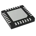
Motor Drivers TMC2209-LA-T QFN-28_L5.0-W5.0-P0.50-BL-EP LCSC Part Number: C2150710 TRINAMIC TMC2209-LA two-phase stepper motor driver IC with STEP/DIR interface, up to 2.8A peak coil current (2A RMS), ultra-quiet StealthChop2 operation, SpreadCycle current control, StallGuard4 sensorless stall detection, CoolStep automatic current reduction, MicroPlyer interpolation up to 256 microsteps, integrated pulse generator, UART configuration interface, internal sense resistor option, low RDS(on) MOSFETs, 4.75V to 29V motor supply range, QFN package with exposed thermal pad, designed for 3D printers, CNC machines, robotics, automation and battery-powered equipment. Search Keywords: TMC2209, TMC2209-LA, Trinamic TMC2209, stepper motor driver, silent stepper driver, StealthChop2, SpreadCycle, StallGuard4, CoolStep, MicroPlyer, UART stepper driver, STEP DIR driver, 2A RMS stepper driver, 2.8A peak motor driver, 3D printer driver, CNC motor driver, QFN stepper driver Hashtags: #TMC2209 #TMC2209LA #Trinamic #StepperDriver #StepperMotorDriver #StealthChop2 #SpreadCycle #StallGuard4 #CoolStep #MicroPlyer #UARTDriver #3DPrinterElectronics #CNCElectronics #MotionControl #MotorDriverIC #SilentStepperDriver
190 Uses1 StarsTLV62569DBVR
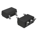
Buck Switching Regulator IC Positive Adjustable 0.6V Output 2A SC-74A, SOT-753 The Texas Instruments TLV62569DBVR is a high-efficiency synchronous step-down (buck) DC-DC converter designed for compact and low-power applications. It converts a higher DC input voltage down to a lower, regulated output voltage with high efficiency and small external component size. It is commonly used in portable electronics, embedded systems, routers, set-top boxes, and battery-powered devices where efficient power conversion and small footprint are important. 🔧 Key Features Input voltage range: 2.5 V to 5.5 V Output current capability: up to 2 A Adjustable output voltage: 0.6 V to VIN (via external resistors) High efficiency: up to ~95% Switching frequency: ~1.5 MHz (allows small inductors/capacitors) Synchronous rectification: improves efficiency by reducing losses Power Save Mode (PSM): boosts efficiency at light load Low quiescent current: ~35 µA typical 100% duty cycle support: low dropout operation 🛡️ Protection & Safety Features Overcurrent protection (OCP) Thermal shutdown protection Internal soft-start (reduces inrush current at startup) Power Good (PG) indicator for system monitoring 📦 Package SOT-23-5 (DBVR) Very small footprint for space-constrained PCB designs ⚙️ Typical Applications Point-of-load (POL) power supplies Wireless routers and networking devices Set-top boxes Battery-powered and portable systems Embedded controllers and IoT devices
157 Uses1 StarsTXS0108EPWR
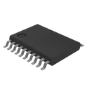
Voltage Level Translator Bidirectional 1 Circuit 8 Channel 60Mbps 20-TSSOP This device is an 8-bit non-inverting level translator which uses two separate configurable power-supply rails. The A port tracks the VCCA pin supply voltage. The VCCA pin accepts any supply voltage between 1.4V and 3.6V. The B port tracks the VCCB pin supply voltage. The VCCB pin accepts any supply voltage between 1.65V and 5.5V. Two input supply pins allows for low Voltage bidirectional translation between any of the 1.5V, 1.8V, 2.5V, 3.3V, and 5V voltage nodes. When the output-enable (OE) input is low, all outputs are placed in the high-impedance (Hi-Z) state. To put the device in the Hi-Z state during power-up or power-down periods, tie OE to GND through a pulldown resistor. The current-sourcing capability of the driver determines the minimum value of the resistor. • No direction-control signal needed • Maximum data rates: – 110Mbps (push pull) – 1.2Mbps (open drain) • 1.4V to 3.6V on A port and 1.65V to 5.5V on B port (VCCA ≤ VCCB) • No power-supply sequencing required – either VCCA or VCCB can be ramped first • Latch-up performance exceeds 100mA per JESD 78, class II • ESD protection exceeds JESD 22 (A port): – 2000 V Human Body Model (A114-B) – 150 V Machine Model (A115-A) – 1000 V Charged-Device Model (C101) • IEC 61000-4-2 ESD (B-port): – ± 8kV Contact Discharge – ± 6kV Air Discharge #commonpartslibrary #integratedcircuit #logic #translator #levelshifter
400 Uses1 Stars
NE555P
The NE555 devices are precision timing circuits capable of producing accurate time delays or oscillation. In time-delay or monostable operating modes, the timed interval is controlled by a single external resistor and capacitor network. In the astable mode of operation, the frequency and duty cycle are controlled independently with two external resistors and a single external capacitor. Each timer has a trigger level equal to approximately one-third of the supply voltage and a threshold level equal to approximately two-thirds of the supply voltage. These levels can be altered by use of the control voltage pin (CONT). When the trigger input (TRIG) is less than the trigger level, the flip-flop is set and the output goes high. If TRIG is greater than the trigger level and the threshold input (THRES) is greater than the threshold level, the flip-flop is reset and the output is low. The reset input (RESET) overrides all other inputs and is used to initiate a new timing cycle. If RESET is low, the flip-flop is reset and the output is low. Whenever the output is low, a lowimpedance path is provided between the discharge pin (DISCH) and the ground pin (GND). Tie all unused inputs to an appropriate logic level to prevent false triggering. The output circuit is capable of sinking or sourcing current up to 200mA. Operation is specified for supplies of 5V to 15V. With a 5V supply, output levels are compatible with TTL inputs. Features - Timing from microseconds to hours - Astable or monostable operation - Adjustable duty cycle - TTL-compatible output can sink or source up to 200mA - On products compliant to MIL-PRF-38535, all parameters are tested unless otherwise noted. Applications - Pulse-shaping circuits - Missing-pulse detectors - Pulse-width modulators - Pulse-position modulators - Sequential timers - Pulse generators -F requency dividers - Industrial controls
2.4k Uses1 Stars