Analog Devices
Analog Devices is a leading provider of high-quality analog and mixed-signal semiconductor solutions for a wide range of applications. From audio and video processing to power management and wireless communication, Analog Devices' extensive portfolio of products helps customers design and build innovative electronic systems with exceptional performance and reliability. If you're looking for comprehensive support in your design process, look no further than Flux.ai. With the world's largest community-driven public library of parts, Flux.ai provides footprints, symbols, datasheets, and simulation models for a wide range of Analog Devices products, making it easy to find the resources you need to get your designs off the ground. So why wait? Start your search for Analog Devices parts today and join the Flux.ai community of design professionals.
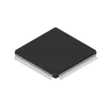
TMS320F280049CPZQR
The TMS320F280049CPZQR is a 32-bit real-time microcontroller from Texas Instruments' C2000 Piccolo family, purpose-built for high-performance digital power control, motor control, and other real-time embedded control applications. The device is centered around TI's C28x digital signal processing core, a fixed- and floating-point architecture specifically optimized for the kind of fast, deterministic mathematical computation required in closed-loop control systems such as motor drives, digital power supplies, solar inverters, and electric vehicle subsystems. This particular part number represents the "C" variant within the TMS320F28004x family, which grants access to an integrated Configurable Logic Block, a flexible programmable logic resource that allows engineers to implement custom digital logic functions directly on-chip, such as specialized PWM waveform shaping, custom protocol interfaces, or glue logic that would otherwise require an external FPGA or discrete logic devices. This variant also provides access to a secure ROM library containing TI's InstaSPIN-FOC technology, a field-oriented motor control solution that significantly simplifies the development of sensorless motor control algorithms by handling much of the underlying control theory and tuning complexity in pre-validated, secure firmware. Beyond its core processing capabilities, the device integrates an extensive set of control-oriented peripherals that are characteristic of the C2000 platform, including high-resolution pulse-width modulation outputs, enhanced capture modules, and a multi-channel sigma-delta filter module that enables isolated current and voltage sensing across an isolation barrier without requiring a separate digital isolator and decoder chip. A dedicated Control Law Accelerator runs in parallel with the main processing core, offloading time-critical control loop calculations so that the main core remains free to handle communication, supervisory logic, and other system-level tasks, which is particularly valuable in systems running multiple simultaneous control loops. Connectivity on the device is supported through a broad set of industry-standard communication interfaces, allowing it to interface with a wide range of external sensors, communication networks, and host systems without requiring additional bridge components. The device also supports TI's Fast Serial Interface, a high-speed, robust communication protocol intended to simplify board-to-board and module-to-module communication in multi-controller systems, an increasingly common need in distributed power and motor control architectures. This part is qualified to automotive electronics reliability standards, making it suitable for deployment in vehicle power electronics, traction inverters, onboard chargers, and other automotive systems where component robustness, extended temperature operation, and rigorous quality screening are required. The device also supports TI's functional safety documentation framework, providing the architectural transparency and failure mode analysis resources needed by system designers building safety-critical control systems around the device. It is housed in a surface-mount package suited to dense power electronics board layouts and is supplied in tape-and-reel packaging for automated assembly. Spec Sheet Identification Part Number: TMS320F280049CPZQR Device Family: C2000 Piccolo, TMS320F28004x Manufacturer: Texas Instruments Variant: "C" type — with Configurable Logic Block and secure ROM/InstaSPIN-FOC access Functional Classification Device Type: 32-bit real-time microcontroller Core Architecture: C28x digital signal processing core Math Acceleration: Floating-Point Unit and Trigonometric Math Unit for control-loop computation Parallel Control Processing: Integrated Control Law Accelerator Programmable Logic: Configurable Logic Block (CLB) for custom digital logic functions Motor Control Library: Secure ROM with InstaSPIN-FOC sensorless field-oriented control Memory Program Memory Type: Embedded flash memory Memory Architecture: Supports field reprogramming for firmware updates and calibration data storage Control & Analog Peripherals PWM Capability: Frequency-independent, high-resolution PWM outputs Capture Module: Enhanced capture (eCAP) peripheral Isolated Sensing: Multi-channel sigma-delta filter module (SDFM) for isolated current/voltage sensing Analog Integration: Integrated high-speed analog-to-digital converters and internal digital-to-analog converters Programmable Gain: Integrated programmable gain amplifiers Communication Interfaces Standard Interfaces: SPI, SCI, I2C, LIN, and CAN connectivity Power Management Bus: Fully compliant PMBus support High-Speed Module Interface: Fast Serial Interface (FSI) for board-to-board and module-to-module communication Target Applications Application Domains: Industrial motor drives, solar inverters, digital power supplies, electric vehicle and transportation systems, sensing and signal processing Environmental & Qualification Automotive Qualification: AEC-Q100 qualified Functional Safety Support: Documentation and architecture support for functional safety-compliant system design Lifecycle Status: Active production Package Package Type: Surface-mount quad flat package style (LQFP) Mounting: Surface mount technology (SMT) Packaging Format Supply Format: Tape-and-reel, per part suffix designation #TMS320F280049 #C2000 #Piccolo #TexasInstruments #DigitalSignalController #RealTimeMCU #MotorControl #DigitalPowerControl #InstaSPINFOC #FieldOrientedControl #ConfigurableLogicBlock #AECQ100 #AutomotiveMCU #PowerElectronics #EmbeddedSystems #LQFP #SurfaceMount #SemiconductorIC #EngineeringSpec #ComponentLibrary #CommonPartsLibrary
3 Uses0 StarsMAX86178
MAX86178 is an ultra-low-power clinical-grade vital-sign analog front-end (AFE) integrating synchronized PPG, single-lead ECG, and BioZ acquisition with I²C interface in a 49-bump WLP package for wearable medical devices. Keywords/Tags: MAX86178, vital-sign AFE, PPG ECG BioZ, wearable health monitor, 49-WLP
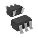
0 Uses0 StarsLP2985IM5X-3.3
Linear Voltage Regulator IC Positive Fixed 1 Output 150mA SOT-23-5 The LP2985IM5X-3.3 specification defines the engineering requirements for a low-dropout linear voltage regulator integrated circuit designed to provide a regulated 3.3 V output for precision analog and digital electronic systems. This specification establishes the functional, electrical, mechanical, thermal, environmental, and quality requirements necessary to ensure stable voltage regulation, low output noise, and long-term operational reliability. The device is intended for use in embedded systems, industrial automation, portable electronics, instrumentation, communication equipment, and battery-powered applications requiring a low-noise and highly stable power supply. Its low dropout voltage, high power supply rejection, and integrated protection features make it suitable for powering microcontrollers, sensors, analog circuitry, and other sensitive electronic devices. Engineering Requirements The low-dropout voltage regulator shall be manufactured using qualified semiconductor fabrication processes and high-quality materials to ensure consistent electrical performance, low quiescent current, and dependable long-term reliability. The device shall maintain stable operation under specified input voltage, output load, temperature, and environmental operating conditions. Electrical characteristics shall provide accurate output voltage regulation, low dropout voltage, excellent line and load regulation, high power supply rejection, and low output noise. The regulator shall maintain stable output performance during startup, shutdown, transient load changes, and supply voltage variations without compromising system operation. The integrated control architecture shall support reliable voltage regulation while incorporating protection mechanisms such as current limiting and thermal shutdown to safeguard both the device and the powered system during abnormal operating conditions. The regulator shall maintain stable performance throughout continuous operation and dynamic load transitions. Thermal performance shall support continuous operation within the specified junction temperature range while maintaining electrical integrity and long-term reliability. The package shall be suitable for automated surface-mount assembly and compatible with standard solder reflow manufacturing processes. Mechanical construction shall withstand thermal cycling, vibration, mechanical handling, and environmental exposure without degradation of electrical or mechanical performance. Workmanship shall be free from defects including contamination, package cracking, bond failures, lead deformation, plating irregularities, or structural inconsistencies that could adversely affect functionality or reliability. Inspection, validation, and testing shall be performed using calibrated equipment and controlled quality procedures to verify compliance with engineering and manufacturing requirements. Any deviation from this specification shall require formal engineering evaluation, documented technical justification, and approval through the established engineering change control process before implementation. Documentation Supporting documentation shall include engineering drawings, electrical performance specifications, thermal characterization reports, application guidelines, qualification records, inspection reports, reliability data, material declarations, and revision-controlled manufacturing documentation. All documentation shall be maintained under formal configuration management and quality assurance systems to ensure complete product traceability. Revision Control Any modification to this specification shall be managed through the formal engineering change management process. All revisions shall undergo technical review, validation, and approval before release to ensure continued compliance with design intent and applicable engineering standards. #EngineeringSpecification #LowDropoutRegulator #LDO #VoltageRegulator #PowerManagement #EmbeddedSystems #IndustrialElectronics #Semiconductor #QualityAssurance #EngineeringDocumentation
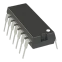
0 Uses0 StarsMCP3204-CI/SL
12 Bit Analog to Digital Converter 2, 4 Input 1 SAR 14-SOIC The MCP3204-CI/SL specification defines the engineering requirements for a multi-channel analog-to-digital converter integrated circuit designed to provide high-accuracy conversion of analog signals into digital data for embedded electronic systems. This specification establishes the functional, electrical, mechanical, thermal, environmental, and quality requirements necessary to ensure precise signal acquisition, reliable data conversion, and long-term operational stability. The device is intended for use in embedded control systems, industrial automation, instrumentation, data acquisition equipment, sensor interfaces, medical electronics, and portable devices requiring accurate analog signal measurement. It supports multiple analog input channels and serial digital communication, enabling efficient integration with microcontrollers and digital processing systems. Engineering Requirements The analog-to-digital converter shall be manufactured using qualified semiconductor fabrication processes and high-quality materials to ensure consistent conversion accuracy, low power consumption, and dependable long-term reliability. The device shall maintain stable operation under specified voltage, temperature, and environmental conditions. Electrical characteristics shall provide accurate analog-to-digital conversion with low noise, excellent linearity, and stable reference performance. The converter shall maintain repeatable sampling characteristics and consistent digital output while supporting reliable serial communication with compatible host controllers. The conversion architecture shall provide predictable sampling behavior, low conversion error, and reliable channel selection while maintaining signal integrity throughout the specified operating range. The device shall support continuous and intermittent data acquisition without degradation of conversion performance. Thermal performance shall support continuous operation within the specified junction temperature range while maintaining electrical characteristics and long-term reliability. The package shall be suitable for automated surface-mount assembly and compatible with standard solder reflow manufacturing processes. Mechanical construction shall withstand thermal cycling, vibration, mechanical handling, and environmental exposure without degradation of functionality. Workmanship shall be free from defects including contamination, package cracking, bond failures, lead deformation, or structural inconsistencies that could adversely affect electrical or mechanical performance. Inspection, validation, and testing shall be performed using calibrated equipment and controlled quality procedures to verify compliance with engineering and manufacturing requirements. Any deviation from this specification shall require formal engineering evaluation, documented technical justification, and approval through the established engineering change control process before implementation. Documentation Supporting documentation shall include engineering drawings, electrical performance specifications, timing diagrams, application guidelines, qualification reports, inspection records, reliability data, material declarations, and revision-controlled manufacturing documentation. All documentation shall be maintained under formal configuration management and quality assurance systems to ensure complete product traceability. Revision Control Any modification to this specification shall be managed through the formal engineering change management process. All revisions shall undergo technical review, validation, and approval before release to ensure continued compliance with design intent and applicable engineering standards. #EngineeringSpecification #AnalogToDigitalConverter #ADC #DataAcquisition #SignalConditioning #EmbeddedSystems #IndustrialElectronics #Semiconductor #QualityAssurance #EngineeringDocumentation
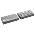
2 Uses0 StarsMSPM0C1104S8YCJR
ARM® Cortex®-M0+ MSPM0 C Microcontroller IC 32-Bit 24MHz 16KB (16K x 8) FLASH 8-DSBGA (0.86x1.6) MSPM0C110x microcontrollers (MCUs) are part of the MSP highly-integrated ultra-low-power 32-bit MCU family based on the enhanced Arm® Cortex®-M0+ core platform operating at up to 24MHz frequency. These costoptimized MCUs offer high-performance analog peripheral integration, support extended temperature ranges from -40°C to 125°C, and operate with supply voltages from 1.62V to 3.6V. The MSPM0C110x devices provide up to 16KB embedded flash program memory with 1KB SRAM. These MCUs incorporate a high-speed on-chip oscillator with an accuracy from -2% to +1.2%, eliminating the need for an external crystal. Additional features include a 1-channel DMA, CRC-16 accelerator, and a variety of highperformance analog peripherals such as one 12-bit 1.5Msps ADC with VDD as the voltage reference, and an on-chip temperature sensor. These devices also offer intelligent digital peripherals such as one 16-bit advanced timer, two 16-bit general purpose timer, one windowed watchdog timer, and a variety of communication peripherals including one UART, one SPI, and one I2C. These communication peripherals offer protocol support for LIN, IrDA, DALI, Manchester, smart card, SMBus, and PMBus. The TI MSPM0 family of low-power MCUs consists of devices with varying degrees of analog and digital integration let customers find the MCU that meets their project needs. The architecture combined with extensive low-power modes is optimized to achieve extended battery life in portable measurement applications. MSPM0C110x MCUs are supported by an extensive hardware and software ecosystem with reference designs and code examples to get the design started quickly. Development kits include a LaunchPad™ kit available for purchase and design files for a target-socket board. TI also provides a free MSP Software Development Kit (SDK), which is available as a component of Code Composer Studio™ IDE desktop and cloud version within the TI Resource Explorer. MSPM0 MCUs are also supported by extensive online collateral, training with MSP Academy, and online support through the TI E2E™ support forums. Features • Core – Arm® 32-bit Cortex®-M0+ CPU, frequency up to 24MHz • Operating characteristics – Extended temperature: –40°C to 125°C – Wide supply voltage range: 1.62V to 3.6V • Memories – Up to 16KB of flash – 1KB of SRAM • High-performance analog peripherals – One analog-to-digital converter (ADC) with up to 10 total external channels, 1.7Msps at 10 bit or 1.5Msps at 12 bit with VDD as the voltage reference – Configurable 1.4V or 2.5V internal ADC voltage reference (VREF) – Integrated temperature sensor – Integrated supply monitor • Optimized low-power modes – RUN: 87µA/MHz – STOP: 609µA at 4MHz, 311µA at 32kHz – STANDBY: 5µA with SRAM retention – SHUTDOWN: 200nA • Intelligent digital peripherals – 1-channel DMA controller dedicated for ADC – Three timers supporting up to 14 PWM channels • One 16-bit advanced timers with deadband support up to 8 PWM channels • One 16-bit general purpose timer with 4 capture/compares • One 16-bit general purpose timer with 2 capture/compares – Windowed watchdog timer – BEEPER generating 1kHz, 2kHz, 4kHz, or 8kHz square wave to drive the external beeper • Enhanced communication interfaces – One UART interface supporting LIN, IrDA, DALI, smart card, Manchester and low-power operation in STANDBY mode – One I2C interface supporting FM+ (1Mbps), SMBus, PMBus, and wakeup from STOP mode – One SPI supporting up to 12Mbps • Clock system – Internal 24MHz oscillator with an accuracy from -2% to +1.2% (SYSOSC) – Internal 32kHz low-frequency oscillator (LFOSC) • Data integrity – Cyclic redundancy checker (CRC-16) • Flexible I/O features – Up to 18 GPIOs – Two 5V-tolerant open-drain IOs • Development support – 2-pin serial wire debug (SWD) • Package options – 20-pin TSSOP (PW) – 20-pin VSSOP (DGS) – 20-pin WQFN (RUK) – 16-pin SOT (DYY) – 8-pin SOT (DDF) – 8-pin WSON (DSG) – 8-pin DSBGA (YCJ) • Family members (also see Device Comparison) – MSPS003F4: 16KB of flash, 1KB of RAM – MSPS003F3: 8KB of flash, 1KB of RAM – MSPM0C1104: 16KB of flash, 1KB of RAM – MSPM0C1103: 8KB of flash, 1KB of RAM • Development kits and software (also see Tools and Software) – LP-MSPM0C1104 LaunchPad™ development kit – MSP Software Development Kit (SDK) 2 Applications • Battery charging and management • Power supplies and power delivery • Personal electronics • Building security and fire safety • Connected peripherals and printers • Grid infrastructure • Smart metering • Communication modules • Medical and healthcare • Lighting #MSPM0C1104S8YCJR #MSPM0C1104 #TexasInstruments #CortexM0Plus #Microcontroller #EmbeddedSystems #LowPowerMCU #IoT #WearableDevices #IndustrialControl #ConsumerElectronics #ADC #UART #SPI #I2C #PWM #TI #ElectronicsDesign #PCBDesign #EmbeddedDevelopment
2 Uses0 StarsSIWG917Y111MGABAR
Bluetooth, WiFi 802.11b/g/n/ax, Bluetooth v5.4 Transceiver Module 2.4GHz Integrated, Chip Surface Mount Silicon Labs SiWG917 module is our lowest power Wi-Fi 6 plus Bluetooth LE 5.4, ideal for ultra-low power IoT wireless devices using Wi-Fi®, Bluetooth, Matter, and IP networking for secure cloud connectivity. It is optimal for developing battery operated devices that need long battery life. SiWG917 module includes an ultra-low power Wi-Fi 6 plus Bluetooth Low Energy (LE) 5.4 wireless CPU subsystem, and an integrated micro-controller (MCU) application subsystem, security, peripherals and power management subsystem all in a single 16 x 21.1 x 2.3 mm package. The wireless subsystem consists of a multi-threaded Network Wireless Processor (NWP) running up to 160 MHz, baseband digital signal processing, analog front end, 2.4 GHz RF transceiver and integrated power amplifier. The application subsystem consists of an ARM® Cortex®-M4 running up to 180 MHz, embedded SRAM, flash, ultra-low power sensor hub, and matrix vector processor. The ARM® Cortex®-M4 is dedicated for peripheral and application-related processing, while the NWP runs the wireless and networking stacks on independent threads, thus providing a fully integrated solution that is ready for a wide range of embedded wireless IoT applications. The modules come with modular radio type approvals for various countries, including USA (FCC), Canada (IC/ISED) and Japan (MIC), and are in compliance with the relevant EN standards (including EN 300 328 v2.2.2) for the conformity with the directives and regulations in EU and UK. KEY FEATURES • Wi-Fi 6 Single Band 2.4 GHz 20 MHz 1x1 stream IEEE 802.11 b/g/n/ax • Bluetooth LE 5.4 • Single chip Matter Over Wi-Fi Solution • ARM® Cortex® M4 Processor with FPU subsystem up to 180 MHz with rich set of Digital and Analog Peripherals. • Wi-Fi 6 Benefits: TWT for improved efficiency and longer battery life, MUMIMO/OFDMA for Higher Throughput, network capacity and low latency • Best in Class Device and Wireless Security • WLAN Tx power up to +17.5 dBm with integrated PA • Bluetooth LE Tx power up to +17 dBm with integrated PA • WLAN Rx sensitivity as low as -95.5 dBm • Wi-Fi 4 Standby Associated mode current: 71 μA @ 1-second listen interval • Embedded Flash option up to 8 MB/ optional external Flash up to 16 MB • Embedded PSRAM option up to 2 MB/ optional external PSRAM option up to 16 MB • Ultra-low power sensor hub peripherals • Matrix Vector Processor (MVP) • Embedded Wi-Fi, Bluetooth LE, Matter, and networking stacks supporting wireless coexistence • Three software-configurable MCU application memory options for sharing the RAM between the wireless, system, and application (192/256/320 KB) • Operating temperature: -40 to +85 ºC • Operating supply range: 3.0 to 3.63 V • Supply voltage for GPIOs: 1.71 to 3.63 V #WiFi6 #BluetoothLE54 #IoTModule #WirelessSoC #SiliconLabs #EmbeddedSystems #SmartHome #IndustrialIoT #LowPowerDesign #RFModule #ConnectedDevices #EdgeComputing #MatterReady #PCBDesign #ElectronicsEngineering
2.2k Uses0 StarsTPS259540DSGT
All details fully confirmed from Texas Instruments' official datasheet, DigiKey, and multiple verified distributor sources. Here's the complete spec. Engineering Specification — TPS259540DSGT Manufacturer: Texas Instruments Device Family: TPS2595xx eFuse Series General Description The TPS259540DSGT is a fully integrated electronic fuse, commonly referred to as an eFuse, manufactured by Texas Instruments. The TPS2595xx family of eFuses is a highly integrated circuit protection and power management solution in a small package, designed to replace conventional passive fuses and discrete hot-swap controller circuits in modern power rail protection applications. Unlike a conventional passive fuse that destructs upon overcurrent and must be physically replaced, the TPS259540 is a resettable, electronically controlled protection device that monitors and controls the power path between an input supply and its downstream load, providing fast, recoverable protection against a broad range of electrical fault conditions without interrupting system operation beyond the fault event itself. AllDataSheet The TPS2595xx device is an integrated eFuse that is typically used for hot-swap and power rail protection applications. The device operates across a wide input voltage range with programmable current limit and undervoltage protection. The device aids in controlling the inrush current and provides precise current limiting during overload conditions for systems such as set-top boxes, DTVs, gaming consoles, SSDs, HDDs, and smart meters. The device also provides robust protection for multiple faults on the sub-system rail. Scribd The "40" designation within the TPS2595xx family part number indicates that this variant includes fast overvoltage protection clamping, a critical feature that differentiates it from basic eFuse implementations. Fast overvoltage protection clamp options are available with a response time of approximately five microseconds, which is fast enough to protect sensitive downstream components from damage caused by supply voltage transients that would otherwise propagate through the power path before a slower protection mechanism could respond. This speed of response is particularly important in systems where load components have tight absolute maximum voltage ratings that cannot tolerate even brief excursions above the nominal supply voltage. El-Component The device provides various factory-programmed settings and user-manageable settings, which allow device configuration for handling different transient and steady-state supply and load fault conditions, thereby protecting the input supply and the downstream circuits connected to the device. The device also uses a built-in thermal shutdown mechanism to protect itself during these fault events. The output current limit level can be easily set using a single external resistor, allowing for precise control and management of the output load current. Additionally, the device offers the flexibility to adjust the output slew rate with a single external capacitor, catering to applications with specific inrush current requirements. ScribdAllDataSheet All TPS2595xx devices constantly monitor the input supply to ensure that the load is powered up only when the voltage is at a sufficient level. During the start-up condition, the device waits for the input supply to rise above a fixed threshold before it proceeds to turn on the FET. Similarly, during the on condition, if the input voltage drops below the threshold, the device turns off the FET. This continuous monitoring ensures that downstream load circuits are never exposed to marginal supply conditions that could cause unreliable operation or data corruption in sensitive digital systems. Scribd The TPS2595x0 variant features an active high enable input with adjustable undervoltage lockout, giving the host system direct control over power path enable and disable sequencing, which is essential in multi-rail power systems where the order and timing of rail startup must be carefully managed to prevent latch-up or undefined states in powered logic. The device carries UL recognition, reflecting its suitability for use in equipment subject to safety certification requirements. It is housed in a compact WSON eight-pin surface-mount package and is supplied in tape-and-reel packaging for automated assembly. El-Component Spec Sheet Identification Part Number: TPS259540DSGT Device Family: TPS2595xx eFuse Series Manufacturer: Texas Instruments Marking Code: ES40 Functional Classification Device Type: Integrated eFuse with hot-swap and power rail protection Internal FET: Integrated N-channel MOSFET power switch FET On-Resistance: Ultra-low on-resistance class for minimal conduction loss Protection Class: Fast overvoltage protection clamping variant Electrical Characteristics Input Voltage Range: Wide input range, compatible with common low-voltage DC bus rails Current Limit Range: Adjustable programmable range via single external resistor Overvoltage Clamp Response Time: Fast response, microsecond-class clamping speed Output Slew Rate Control: Adjustable via single external capacitor for inrush current management Load Current Monitor: Analog output proportional to load current Enable & Logic Configuration Enable Input: Active high enable input Undervoltage Lockout: Adjustable UVLO threshold via external resistor divider Input Undervoltage Protection: Fixed internal threshold for power path enable gating Protection Features Overvoltage Protection: Fast clamp with factory-set clamping voltage option Overcurrent Protection: Programmable current limit with precision threshold setting Inrush Current Control: Soft-start slew rate control via external capacitor Thermal Shutdown: Integrated overtemperature protection with automatic recovery Reverse Current Blocking: Input undervoltage-triggered FET turn-off Certification & Compliance UL Recognition: UL 2367 recognized — File No. E169910 Export Classification: EAR99 RoHS Compliance: Yes Target Applications Hot-swap power path management Power rail protection for set-top boxes, gaming consoles, and smart meters SSD and HDD power management Digital TV and consumer AV subsystem power protection Industrial multi-rail power sequencing IoT and embedded system power protection Package Package Type: WSON — Small Outline No-Lead, eight-pin Package Designation: DSG suffix Mounting Method: Surface mount technology (SMT) Packaging Format Supply Format: Tape-and-reel — DSGT suffix #TPS259540 #TPS2595xx #TexasInstruments #eFuse #HotSwap #PowerRailProtection #OvervoltageProtection #CurrentLimit #InrushControl #PowerManagement #WSON #SurfaceMount #IntegratedFET #CircuitProtection #PowerSequencing #SmartPower #SemiconductorIC #EngineeringSpec #ComponentLibrary #CommonPartsLibrary #RoHSCompliant #ULRecognized
10 Uses0 StarsPAM8403DR
Amplifier IC 2-Channel (Stereo) Class D 16-SOP PAM8403 mini amplifier module The PAM8403DR is a filterless Class-D stereo audio amplifier IC manufactured by Diodes Incorporated, designed to deliver efficient, high-quality audio amplification in compact, battery-powered, and USB-powered consumer electronics. The device integrates two independent amplifier channels within a single integrated circuit, providing a complete stereo audio power amplification solution without requiring significant external passive components, making it one of the most widely used Class-D audio amplifier ICs in the consumer and embedded electronics market. AllDataSheet The Class-D amplification topology used in this device operates by switching the output stage rapidly between supply rail voltage states rather than linearly driving an analog output signal, resulting in significantly higher power conversion efficiency than traditional Class-AB amplifiers. This high efficiency means that the vast majority of the power drawn from the supply is delivered to the speaker loads rather than being dissipated as heat within the IC itself, which is critical in battery-powered applications where minimizing power consumption extends operating time, and in compact enclosures where thermal management is constrained. The filterless architecture allows the device to drive the speaker directly, requiring no low-pass output filters, thus saving system cost and PCB area. In conventional Class-D amplifiers, the high-frequency switching content in the output must be removed by a passive LC output filter before the signal can be applied to a speaker, adding component cost and board footprint. The PAM8403's filterless design achieves its output filtering effect through the natural inductance of the speaker voice coil itself, eliminating the external filter requirement entirely in most applications while maintaining low distortion and good audio fidelity. AllDataSheet The device incorporates protection circuitry to safeguard both itself and the connected speaker loads from fault conditions that can arise during normal use, including output short-circuit events, excessive junction temperature caused by high ambient temperature or heavy output loading, and supply voltage conditions outside the normal operating range. These protection features allow the device to recover automatically from transient fault conditions without damage or requiring manual reset, improving system reliability and reducing the risk of speaker or amplifier damage in consumer products. The device supports a wide range of load impedances, making it compatible with the majority of commonly used small speaker drivers found in portable electronics, desktop multimedia systems, educational devices, and embedded audio applications. Its wide supply voltage operating range makes it directly compatible with USB bus power, single-cell lithium-ion battery power, and regulated supply rails commonly found in embedded system designs. The PAM8403DR is supplied in a compact surface-mount small-outline package on tape-and-reel packaging suitable for automated assembly, with construction compliant to RoHS material restrictions. Note that DigiKey currently lists this part as obsolete, though the device remains available through other distribution channels. Spec Sheet Identification Part Number: PAM8403DR Device Family: PAM8403 Manufacturer: Diodes Incorporated Functional Classification Device Type: Stereo Class-D audio power amplifier IC Amplifier Topology: Class-D switching amplifier Number of Channels: Dual channel, stereo Output Architecture: Filterless, direct speaker drive Electrical Characteristics Supply Voltage Range: Wide-range supply, compatible with USB bus power and single-cell lithium battery rails Output Power Class: Low-watt stereo class, suitable for small speaker drivers Output Load Impedance: Compatible with standard small speaker load impedances Audio Quality: Low total harmonic distortion plus noise for high-quality sound reproduction Efficiency: High efficiency class-D conversion, low heat dissipation Protection Features Short-Circuit Protection: Integrated output short-circuit protection Thermal Shutdown: Automatic overtemperature protection with recovery Undervoltage Lockout: Supply undervoltage detection and output disable EMI Management Filterless Operation: Speaker voice coil inductance acts as output filter Optional EMI Mitigation: Ferrite bead filter on speaker traces recommended for long trace lengths to reduce high-frequency EMI radiation Environmental & Qualification Operating Temperature Range: Extended industrial range RoHS Compliance: Yes Lifecycle Status: Obsolete at DigiKey; available through alternate distribution channels Package Package Type: Small-outline IC package, SOP-style Mounting: Surface mount technology (SMT) Packaging Format Supply Format: Tape-and-reel #PAM8403 #PAM8403DR #DiodesIncorporated #ClassDAmp #AudioAmplifier #StereoAmp #FilterlessClassD #PowerAmplifier #AudioIC #CompactAudio #USBPowered #BatteryPowered #PortableAudio #EmbeddedAudio #ConsumerElectronics #SOIC #SurfaceMount #SemiconductorIC #EngineeringSpec #ComponentLibrary #CommonPartsLibrary #RoHSCompliant #commonpartslibrary #integratedcircuit #amplifier
143 Uses0 StarsHSCDRRN001ND2A5
Pressure Sensor ±0.04PSI (±0.25kPa) Differential Male - 0.08" (1.93mm) Tube, Dual 12 b 8-DIP (0.524", 13.30mm), Dual Ports, Same Side Excellent — full picture confirmed from multiple sources. The HSCDRRN001ND2A5 is a TruStability HSC Series high accuracy digital I²C sensor with address 0x28, DIP package, dual radial barbed ports on the same side, differential pressure type, rated for ±1 inH₂O, operating on a 5.0 Vdc supply. Here's the complete spec. HIROSE Electric Engineering Specification — HSCDRRN001ND2A5 Manufacturer: Honeywell Sensing and Productivity Solutions Device Family: TruStability HSC Series General Description The HSCDRRN001ND2A5 is a high-accuracy, fully compensated and amplified differential pressure sensor manufactured by Honeywell, belonging to the TruStability HSC Series of board-mount pressure sensing devices. The device is built around a piezoresistive silicon sensing element housed within a ceramic package, combining a mature and proven sensing principle with advanced on-chip signal conditioning that makes the device ready for direct interfacing with a host microcontroller or processor without requiring extensive external analog signal processing circuitry. The defining characteristic of the TruStability HSC series, and of this device in particular, is its fully calibrated and temperature-compensated output, achieved through an integrated application-specific integrated circuit that corrects for sensor offset, sensitivity drift, temperature effects, and pressure nonlinearity across the device's rated operating range. This level of factory compensation allows the device to maintain its specified accuracy across the full compensated temperature range without requiring individual board-level calibration, significantly simplifying the design and production process for equipment that relies on precise low-pressure measurement. This particular configuration uses a digital I²C output interface, communicating pressure readings as high-resolution digital data words over a standard two-wire bus using a fixed I²C device address. This digital output makes it highly compatible with modern embedded system architectures where analog-to-digital conversion resources may be limited or where noise immunity and data integrity over longer trace runs are priorities. The device offers both high resolution and high accuracy within a tight total error band, making it suitable for applications where small differential pressure differences must be resolved reliably over time and temperature variation. The sensor is configured as a differential pressure measurement device, meaning it produces an output proportional to the difference in pressure between its two pneumatic ports rather than to absolute or gauge pressure relative to atmosphere. This makes it particularly well suited to airflow measurement, filter condition monitoring, liquid level detection, spirometry and respiratory measurement, HVAC duct pressure sensing, and other applications where the pressure difference across two points in a system is the relevant physical quantity. The device is housed in a through-hole dual in-line package with two radial barbed pneumatic port fittings located on the same side of the package body, allowing small-bore flexible tubing to be connected directly to each port without requiring additional adapter fittings. The barbed port design provides a secure, friction-held tube connection that resists accidental disconnection during normal handling and operation. The package is designed for standard through-hole PCB mounting, and the device is intended for use with non-corrosive, non-ionic dry gases only, consistent with the silicon and ceramic wetted materials used in its construction. Spec Sheet Identification Part Number: HSCDRRN001ND2A5 Series: TruStability HSC Series Manufacturer: Honeywell Sensing and Productivity Solutions Functional Classification Device Type: Board-mount piezoresistive silicon pressure sensor Sensing Type: Differential pressure Compensation: Fully calibrated and temperature compensated via integrated ASIC Accuracy Class: High accuracy, tight total error band class Output Interface Output Type: Digital I²C I²C Device Address: Fixed address 0x28 Output Resolution: High-resolution digital pressure word Applicable Interface Standards: I²C-compatible digital output Pressure Port Configuration Port Style: Dual radial barbed ports Port Orientation: Same side, both ports on the same face of the package Tubing Connection: Direct small-bore flexible tube connection via barbed fittings Media Compatibility: Non-corrosive, non-ionic dry gases only Pressure Characteristics Pressure Type: Differential Pressure Range: Very low differential pressure class, sub-inch water column range Overpressure Capability: Rated overpressure withstand above operating range Power Supply Supply Voltage: Standard logic-level supply rail class Environmental & Mechanical Operating Temperature Range: Commercial/industrial extended temperature range Compensated Temperature Range: Subset of the full operating temperature range, within which calibrated accuracy is maintained Mount Type: Through-hole Package: DIP (Dual In-line Package), standard pin pitch Application Suitability Target Applications: Airflow measurement, HVAC duct pressure sensing, filter monitoring, respiratory and spirometry equipment, liquid level detection, low-pressure process monitoring Environmental & Qualification RoHS Compliance: Yes Media Restriction: Dry, non-corrosive, non-ionic gases only; no liquid media on Port #HSCDRRN001ND2A5 #Honeywell #TruStability #HSCSeries #PressureSensor #DifferentialPressure #PiezoresistiveSensor #I2CSensor #BoardMountSensor #LowPressureSensor #AirflowSensor #HVACSensor #RespiratoryMedical #ThroughHole #DIPPackage #CompensatedSensor #TemperatureCompensated #SensorDatasheet #EngineeringSpec #ComponentLibrary #CommonPartsLibrary #RoHSCompliant
0 Uses0 StarsMCP6004-E/P
MCP6001/MCP6002/MCP6004 are low-power rail-to-rail input/output operational amplifiers from Microchip Technology designed for battery-powered, portable, industrial, automotive, and general-purpose analog applications. Operating from a single supply voltage of 1.8 V to 6.0 V, the family provides a typical gain-bandwidth product of 1 MHz, low quiescent current of only 100 µA per amplifier, and full rail-to-rail input/output operation for maximum dynamic range. Available in single, dual, and quad amplifier versions, the MCP600x series is well suited for sensor interfaces, photodiode amplifiers, analog filters, signal conditioning, portable instrumentation, IoT devices, battery-powered electronics, and embedded analog circuits requiring low power consumption and cost-effective performance. Search Keywords: MCP6001, MCP6002, MCP6004, Microchip MCP6001, Rail to Rail Op Amp, Low Power Operational Amplifier, Single Supply Op Amp, General Purpose Op Amp, Analog Signal Conditioning, Sensor Amplifier, Photodiode Amplifier, Battery Powered Amplifier, Low Voltage Op Amp, 1MHz Op Amp, Rail to Rail Input Output Amplifier, Portable Electronics Amplifier, Embedded Analog Circuit, Analog Filter Amplifier, Precision Signal Amplifier, Microchip Operational Amplifier Hashtags: #MCP6001 #MCP6002 #MCP6004 #Microchip #OperationalAmplifier #OpAmp #RailToRail #AnalogElectronics #SignalConditioning #SensorInterface #LowPowerDesign #BatteryPowered #EmbeddedSystems #AnalogCircuit #ElectronicsDesign #PCBDesign #HardwareEngineering #IoTDevices #Instrumentation #ElectricalEngineering
2 Uses0 Stars