Transistors
A transistor is a type of electronic device that controls the flow of electricity or current through a circuit. It acts as a switch or gate, allowing current to pass through or blocking it, depending on the input signal applied to the transistor. Transistors are widely used in a variety of electronic devices and systems, including computers, televisions, radios, and smartphones. They are also used in a range of industrial and medical applications, such as power supply systems and medical equipment. Flux.ai is home to the world's largest community-driven public library of transistors, with footprints, symbols, datasheets, and simulation models available for a wide range of devices. The library is constantly being updated and expanded by a community of engineers and enthusiasts, making it an invaluable resource for anyone working with transistors. Whether you're a student, hobbyist, or professional engineer, you'll find everything you need to know about transistors at Flux.ai.
EPC2019
GANFET N-CH 200V 8.5A DIE The EPC2019 is an enhancement-mode N-channel Gallium Nitride (eGaN®) power transistor designed for high-speed and high-efficiency power conversion applications. With a 200 V drain-to-source voltage rating, 42 mΩ maximum RDS(on), and 8.5 A continuous drain current, it offers significantly lower switching losses than conventional silicon MOSFETs. Its ultra-low gate charge, zero reverse recovery charge (QRR), and fast switching characteristics make it ideal for high-frequency switching circuits. The device is supplied in a bare die (passivated die with solder bars) package for optimized thermal and electrical performance in compact, high-density designs. Key Features Enhancement-mode N-channel eGaN® FET 200 V drain-to-source voltage (VDS) 42 mΩ maximum RDS(on) @ VGS = 5 V 8.5 A continuous drain current Ultra-low gate charge (Qg ≈ 2.9 nC) Zero reverse recovery charge (QRR) for reduced switching losses Supports high-frequency switching operation Gate drive compatible with 0 V OFF / 5 V ON (no negative gate voltage required) Bare die package for compact, high-performance power designs Operating junction temperature: −40°C to +150°C #EPC2019 #eGaN #GaNFET #PowerTransistor #NChannelFET #HighEfficiency #HighSpeedSwitching #PowerElectronics #DCDCConverter #ClassDAudio #EfficientPowerConversion
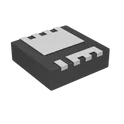
6 Uses0 StarsBSC030N10NS5SCATMA1
N-Channel 100 V 171A (Tc) 188W (Tc) Surface Mount PG-WSON-8-2 The BSC030N10NS5SCATMA1 specification defines the engineering requirements for an N-channel power MOSFET designed for high-efficiency switching and power management applications. This specification establishes the functional, electrical, mechanical, thermal, environmental, and quality requirements necessary to ensure reliable switching performance, low conduction losses, and long-term operational stability in power electronic systems. The device is intended for use in DC-DC converters, synchronous rectification circuits, motor control systems, battery management systems, power distribution modules, and industrial electronic equipment. It provides low on-state resistance, fast switching characteristics, and efficient power handling, making it suitable for high-frequency and high-current applications requiring optimized efficiency and thermal performance. Engineering Requirements The power MOSFET shall be manufactured using advanced semiconductor fabrication processes and qualified materials to ensure consistent electrical characteristics, high switching efficiency, and reliable long-term operation. The device shall maintain stable performance under specified voltage, current, and environmental operating conditions. Electrical characteristics shall provide low on-state resistance, high current-carrying capability, low gate charge, and fast switching performance to minimize conduction and switching losses. The device shall maintain stable operation during repetitive switching cycles, transient load conditions, and dynamic power management applications. Thermal performance shall support efficient heat dissipation through the package structure and printed circuit board interface. The component shall maintain electrical integrity and operational reliability within the specified junction temperature range during continuous and intermittent high-power operation. Mechanical construction shall be suitable for automated surface-mount assembly and compatible with standard solder reflow manufacturing processes. The package shall withstand vibration, thermal cycling, mechanical handling, and environmental exposure without degradation of electrical or mechanical performance. Workmanship shall be free from defects including contamination, cracks, bond failures, package deformation, or structural inconsistencies. Inspection, validation, and testing shall be conducted using calibrated equipment and controlled quality procedures to verify compliance with all applicable engineering and manufacturing requirements. Any deviation from this specification shall require formal engineering evaluation, documented technical justification, and approval through the established engineering change control process. Documentation Supporting documentation shall include engineering drawings, electrical performance specifications, thermal characterization reports, qualification records, inspection reports, material declarations, reliability data, and revision-controlled manufacturing documentation. All documentation shall be maintained under formal configuration management and quality assurance systems to ensure complete product traceability. Revision Control Any modification to this specification shall be managed through the formal engineering change management process. All revisions shall undergo technical review, validation, and approval before implementation to ensure continued compliance with design intent and applicable engineering standards. #EngineeringSpecification #PowerMOSFET #NChannelMOSFET #PowerElectronics #PowerManagement #MotorControl #DCDCConverter #Semiconductor #QualityAssurance #EngineeringDocumentation #commonpartslibrary #transistor #mosfet
0 Uses0 StarsRGPR20NS43HRTL
IGBT 460 V 20 A 107 W Surface Mount LPDS #CommonPartsLibrary #Transistor #IGBT The RGPR20NS43HRTL specification defines the engineering requirements for an ultrafast recovery power rectifier designed for high-efficiency power conversion and switching applications. This specification establishes the functional, electrical, mechanical, thermal, environmental, and quality requirements necessary to ensure reliable rectification performance, low switching losses, and long-term operational stability in power electronic systems. The device is intended for use in switch-mode power supplies, power factor correction circuits, motor drives, industrial power equipment, and other high-frequency power conversion applications. It provides efficient current rectification with fast reverse recovery characteristics, enabling improved system efficiency and reduced electromagnetic interference in demanding electrical environments. Engineering Requirements The rectifier shall be manufactured using qualified semiconductor fabrication processes and high-quality materials to ensure consistent electrical performance, thermal stability, and long service life. The device shall maintain reliable operation under specified voltage, current, and temperature conditions without degradation of functional performance. Electrical characteristics shall provide low forward voltage drop, fast reverse recovery time, and high surge current capability to support efficient high-frequency switching applications. The device shall maintain stable electrical behavior under repetitive switching cycles and transient operating conditions. Thermal performance shall support effective heat dissipation through the package structure and recommended mounting configuration. The component shall operate within specified junction temperature limits while maintaining electrical integrity and long-term reliability under continuous or intermittent load conditions. Mechanical construction shall be suitable for standard surface-mount or through-hole assembly, depending on the package configuration, and shall withstand soldering, handling, vibration, and thermal cycling without mechanical degradation. Workmanship shall be free from defects including contamination, cracks, bond failures, corrosion, or structural inconsistencies that could adversely affect electrical or mechanical performance. Inspection, validation, and testing shall be conducted using calibrated equipment and controlled quality procedures to verify compliance with all applicable engineering and manufacturing requirements. Any deviation from this specification shall require formal engineering evaluation, documented technical justification, and approval through the established engineering change control process. Documentation Supporting documentation shall include engineering drawings, electrical performance data, thermal characterization reports, qualification records, inspection reports, and revision-controlled manufacturing documentation. All documentation shall be maintained under formal configuration management and quality assurance systems to ensure complete product traceability. Revision Control Any modification to this specification shall be managed through the formal engineering change management process. All revisions shall undergo technical review, validation, and approval before implementation to ensure continued compliance with design intent and applicable engineering standards. #EngineeringSpecification #PowerRectifier #UltrafastRecoveryDiode #PowerElectronics #SwitchModePowerSupply #IndustrialElectronics #Semiconductor #ThermalManagement #QualityAssurance #EngineeringDocumentation
0 Uses0 StarsDRV8770RGER
Half Bridge (2) Driver DC Motors, General Purpose NMOS, Power MOSFET 24-VQFN (4x4) The DRV8770RGER is a high-voltage brushed DC motor gate driver integrated circuit manufactured by Texas Instruments, designed to drive external N-channel power MOSFETs configured in a dual half-bridge topology for use in brushed DC motor control, stepper motor drive, solenoid actuation, and other inductive load switching applications. Rather than integrating the power stage transistors directly within the IC, the DRV8770 functions as a gate driver, providing the gate voltage and current needed to fully and rapidly switch external discrete power MOSFETs, which allows the designer to choose power devices appropriate to the specific voltage and current requirements of their motor or load without being constrained by the internal power stage of an integrated motor driver. The DRV8770 delivers two half-bridge gate drivers, each capable of driving high-side and low-side N-channel power MOSFETs. The integrated bootstrap diode and external capacitor generate the correct gate drive voltages for the high-side MOSFETs, while the GVDD rail drives the gates of the low-side MOSFETs. This bootstrap architecture eliminates the need for an external isolated gate drive power supply for the high-side switch, simplifying the overall power stage design significantly compared to approaches that require separate high-side power supply generation. This device decreases system component count, reduces PCB area, and saves cost by integrating two independent half-bridge gate drivers and bootstrap diodes. digikeyTME The high-side and low-side gate drivers can drive source and sink currents sufficient for fast, efficient switching of external power MOSFETs, with total average output current capability defined in the datasheet. The asymmetric source and sink current capability is a deliberate design choice reflecting the typical requirements of power MOSFET switching, where rapid turn-off is often more critical than turn-on speed for preventing shoot-through and managing switching losses in bridge circuits. Small propagation delay and delay matching specifications minimize the dead-time requirement, which further improves efficiency. TMEFarnell The high voltage tolerance of the gate drive pins improves system robustness. The SHx phase pins can tolerate significant negative voltage transients, while the high-side gate driver supply can support higher positive voltage transients on the BSTx and GHx pins. This enhanced transient tolerance is essential in motor drive applications where inductive switching generates voltage spikes and negative voltage excursions on the switch node that would damage less robust gate driver designs. An input deglitcher prevents high-frequency noise on the input pins from affecting the output state of the gate drivers, protecting against inadvertent switching caused by electrical noise on the control interface lines. FarnellAllDataSheet The device can drive one or two DC brush motors, one stepper motor, solenoids, or other inductive loads. This versatility makes it suitable across a broad range of actuator types within the same hardware platform, allowing a single PCB design to serve multiple product variants by simply changing the connected load and the firmware control scheme. Undervoltage protection is provided for both low-side and high-side through GVDD and BST undervoltage lockout, preventing the external power MOSFETs from operating with insufficient gate drive voltage, which would cause them to enter a linear operating region with excessive power dissipation and potential thermal damage. digikeyFarnell The DRV8770RGER is housed in a compact VQFN twenty-four-pin surface-mount package, suited to space-constrained motor drive PCB layouts, and is rated for operation across an extended industrial temperature range. Spec Sheet Identification Part Number: DRV8770RGER Device Family: DRV8770 Manufacturer: Texas Instruments Functional Classification Device Type: Dual half-bridge N-channel MOSFET gate driver IC Topology: Two independent half-bridge gate drivers Application Class: Brushed DC motor, stepper motor, solenoid, and inductive load drive Gate Drive Architecture High-Side Driver: Bootstrap-based gate drive with integrated bootstrap diode Low-Side Driver: GVDD-referenced direct gate drive Gate Drive Current — Source: High source current capability for rapid MOSFET turn-on Gate Drive Current — Sink: Higher sink current capability for rapid MOSFET turn-off Voltage Ratings Maximum Operating Voltage: High-voltage class, suited to industrial motor supply rails Phase Pin Transient Tolerance: Rated for negative voltage transients on SHx switch node pins Bootstrap Pin Transient Tolerance: Elevated absolute maximum on BSTx and GHx pins for spike immunity Timing & Switching Performance Propagation Delay: Small and tightly specified for minimal dead-time requirement Delay Matching: High-side to low-side delay matching for improved bridge efficiency Input Deglitching: Built-in input deglitch filter to suppress high-frequency noise on control inputs Protection Features GVDD Undervoltage Lockout: Protects low-side gate drive from insufficient supply BST Undervoltage Lockout: Protects high-side gate drive from insufficient bootstrap voltage Negative Transient Tolerance: Phase pins rated for switch-node negative voltage excursions Load Compatibility Supported Load Types: Brushed DC motors, stepper motors, solenoids, and general inductive loads Drive Configurations: Single or dual brushed DC motor, single stepper motor, or independent half-bridge loads Environmental & Qualification Operating Temperature Range: Extended industrial temperature range RoHS Compliance: Yes Lifecycle Status: Active production Package Package Type: VQFN — Very thin Quad Flat No-Lead, twenty-four-pin Package Suffix: RGER designation Mounting Method: Surface mount technology (SMT) Package Pitch: Fine pitch, compact footprint Packaging Format Supply Format: Tape-and-reel, cut-tape, and custom reel options available #DRV8770 #DRV8770RGER #TexasInstruments #GateDriver #HalfBridgeDriver #BrushedDCMotor #MotorDriver #StepperMotorDriver #SolenoidDriver #NChannelMOSFET #BootstrapDriver #HighVoltageDriver #PowerElectronics #MotorControl #InductiveLoad #VQFN #SurfaceMount #SemiconductorIC #EngineeringSpec #ComponentLibrary #CommonPartsLibrary #RoHSCompliant #IndustrialMotorDrive
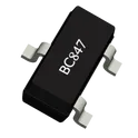
2 Uses0 StarsBC847
All details fully confirmed across multiple authoritative sources including Nexperia, ROHM, Farnell, and others. Here's the complete spec. Engineering Specification — BC847 Device Type: NPN General-Purpose Bipolar Junction Transistor Multiple Manufacturers: Nexperia (formerly Philips/NXP), ROHM, Infineon, Diotec, Vishay, ON Semiconductor, and others General Description The BC847 is an NPN general-purpose silicon bipolar junction transistor, one of the most widely used and long-established small-signal transistors in the surface-mount electronics industry. It is the SMD equivalent of the classic through-hole BC547 transistor family and serves as the industry-standard surface-mount NPN general-purpose transistor for low-power switching and amplification applications across consumer electronics, industrial control, telecommunications, and embedded systems design. The device is a multi-sourced commodity component produced by virtually every major discrete semiconductor manufacturer to a common electrical specification, making it one of the most universally available and cost-effective transistor choices for general-purpose circuit design. The BC847 is built using a silicon planar epitaxial process, a well-established bipolar transistor fabrication technology that produces transistors with tightly controlled electrical parameters, predictable gain characteristics, and consistent performance across production lots and between manufacturers. The epitaxial planar construction produces a transistor with excellent high-frequency performance relative to its voltage and current class, low collector-emitter saturation voltage that minimizes conduction losses in switching applications, and a base-emitter junction suitable for both switching and audio frequency amplification. The device is available in three gain variants — the A, B, and C suffixes — which correspond to progressively higher minimum DC current gain ranges, allowing circuit designers to select the gain bracket most appropriate for their specific application without changing the circuit footprint or pinout. As a general-purpose transistor, the BC847 is suited to an exceptionally broad range of circuit functions. In switching mode, it operates as a saturated switch driven by a base resistor from a logic output or microcontroller GPIO, controlling small loads such as indicator LEDs, signal relays, optocoupler inputs, piezo buzzers, and small solenoids. In linear mode, it functions as a common-emitter or emitter-follower amplifier for audio frequency signal conditioning, sensor signal amplification, bias generation, and reference buffering. Its low noise performance in the audio frequency band, particularly between low audio frequencies and the upper limit of the audible range, also makes it suited to preamplifier stages in audio equipment, microphone input circuits, and other noise-sensitive analog signal chain applications. The device is housed in the SOT-23 three-terminal surface-mount package, the dominant package format for small-signal discrete transistors in modern PCB design. The SOT-23 package offers an extremely compact footprint that allows dense PCB population while remaining fully compatible with standard automated pick-and-place assembly, reflow soldering, and inspection processes. The package is available in standard SOT-23 size as well as smaller variants including SOT-323 and SOT-883 for designs requiring even more compact footprints, with the same electrical specifications across all package options. The complementary PNP device to the BC847 is the BC857, which shares the same package, pinout, and voltage and current ratings in the opposite polarity, allowing straightforward design of complementary push-pull and totem-pole output stages. Spec Sheet Identification Part Number: BC847 (suffixes A, B, C denote gain groups) Device Family: BC847 series, NPN general-purpose transistor Manufacturer: Multi-sourced commodity part — Nexperia, ROHM, Infineon, Diotec, Vishay, ON Semiconductor, and others PNP Complement: BC857 Functional Classification Device Type: NPN bipolar junction transistor (BJT) Construction: Silicon planar epitaxial Application Class: General-purpose switching and amplification Gain Variants BC847A: Lowest gain range group BC847B: Mid gain range group BC847C: Highest gain range group Absolute Maximum Ratings Collector-Emitter Voltage: Standard low-voltage small-signal transistor class Collector-Base Voltage: Slightly higher than collector-emitter rating Emitter-Base Voltage: Standard emitter-base reverse voltage class Collector Current: Low continuous current class, suitable for signal and small load switching Peak Collector Current: Higher pulsed current capability Total Power Dissipation: Low power dissipation class, standard for SOT-23 package Operating Junction Temperature: Extended range, standard silicon transistor class Electrical Characteristics DC Current Gain: Variant-dependent, high gain class for general-purpose applications Collector-Emitter Saturation Voltage: Low saturation voltage for efficient switching Base-Emitter Saturation Voltage: Standard silicon junction voltage class Collector Cutoff Current: Low leakage class Transition Frequency: High-frequency capable for audio and signal switching applications Noise Figure: Low noise in audio frequency band Package & Mechanical Primary Package: SOT-23 (TO-236AB) Alternate Packages: SOT-323 (SC-70), SOT-883 (DFN1006-3) — same electrical specs Mounting Method: Surface mount technology (SMT) Pin Configuration: Base — Pin 1, Emitter — Pin 2, Collector — Pin 3 Target Applications Logic-level switching of LEDs, relays, and small loads Audio frequency signal amplification and preamplification Sensor signal conditioning and buffering Emitter follower and bias circuits Optocoupler and interface drive circuits General-purpose analog and digital circuit design Environmental & Qualification RoHS Compliance: Yes, lead-free across all manufacturer sources Flammability Rating: UL94 V-0 package material Packaging Supply Format: Tape-and-reel, per manufacturer standard packaging #BC847 #BC847B #BC847C #NPNTransistor #BipolarTransistor #BJT #SmallSignalTransistor #GeneralPurposeTransistor #SOT23 #SurfaceMountTransistor #SwitchingTransistor #AmplifierTransistor #LowPowerTransistor #SiliconEpitaxial #BC857Complement #DiscreteComponent #AnalogCircuit #EmbeddedSystems #EngineeringSpec #ComponentLibrary #CommonPartsLibrary #RoHSCompliant #CommodityPart
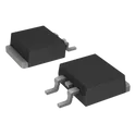
14 Uses0 StarsMC7805CTG
Linear Voltage Regulator IC Positive Fixed 1 Output 1A TO-220 These voltage regulators are monolithic integrated circuits designed as fixed−voltage regulators for a wide variety of applications including local, on−card regulation. These regulators employ internal current limiting, thermal shutdown, and safe−area compensation. With adequate heatsinking they can deliver output currents in excess of 1.0 A. Although designed primarily as a fixed voltage regulator, these devices can be used with external components to obtain adjustable voltages and currents. Features • Output Current in Excess of 1.0 A • No External Components Required • Internal Thermal Overload Protection • Internal Short Circuit Current Limiting • Output Transistor Safe−Area Compensation • Output Voltage Offered in 1.5%, 2% and 4% Tolerance • Available in Surface Mount D2PAK−3, DPAK−3 and Standard 3−Lead Transistor Packages • NCV Prefix for Automotive and Other Applications Requiring Unique Site and Control Change Requirements; AEC−Q100 Qualified and PPAP Capable • These are Pb−Free Devices #MC7805CTG #7805 #VoltageRegulator #LinearRegulator #PowerManagement #5VRegulator #Onsemi #TO220 #EmbeddedSystems #ElectronicsDesign #PowerSupply #PCBDesign #HardwareEngineering #IndustrialElectronics #CircuitDesign
21 Uses0 Stars