Memory
A memory IC, or integrated circuit, is a type of electronic device that stores and retrieves data. It is used in a wide range of electronic devices, including computers, smartphones, and other electronic devices. Memory ICs come in a variety of types, including DRAM, SRAM, and Flash memory, and are used for different purposes depending on the device and application. One of the primary use cases for memory ICs is in computer systems, where they are used to store data and instructions that are accessed by the processor. Memory ICs are also used in a variety of other electronic devices, such as digital cameras, MP3 players, and mobile phones, to store data and enable various functions. Flux.ai has the world's largest community-driven public library of memory ICs, with a wide variety of footprints, symbols, datasheets, and simulation models available. This extensive library allows users to easily access and use memory ICs in their projects, making it an invaluable resource for engineers and developers.
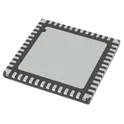
EFR32ZG23B020F512IM48-B
IC RF TxRx + MCU General ISM < 1GHz Z-Wave® 863MHz ~ 870MHz, 902MHz ~ 928MHz 48-VFQFN Exposed Pad The Silicon Labs EFR32ZG23B020F512IM48-B is a 2.4 GHz–independent (sub-GHz) RF Tx/Rx + MCU SoC optimized for Z-Wave smart home and IoT mesh networks. It integrates computing, RF communication, and security features in a compact 48-pin QFN package. It is part of the EFR32ZG23 Series 2 platform, which focuses on low-power, secure, long-range wireless connectivity for smart home, building automation, and industrial IoT devices. Key Features MCU Core & Memory ARM Cortex-M33 core (up to ~80 MHz) 512 kB Flash memory 64 kB RAM RF / Wireless Z-Wave protocol support (mesh + long-range) Frequency bands: 863–870 MHz (EU) 902–928 MHz (US) Max data rate: up to 100 kbps Output power: up to +20 dBm High sensitivity: around –110 dBm Security Secure Vault™ high-level security subsystem Hardware cryptography support Secure boot and key protection (IoT-grade security) Low Power Performance Ultra-low receive and transmit currents (single-digit mA RX, tens of mA TX) Designed for battery-powered IoT nodes Peripherals & Interfaces GPIO (up to ~31 pins depending on variant) ADC, I2C, SPI, UART, I2S, IrDA Flexible digital/analog peripheral integration Package & Electrical 48-pin QFN (6 × 6 mm) Supply voltage: 1.71 V – 3.8 V Industrial temperature range: –40°C to +125°C #CommonPartsLibrary #IntegratedCircuit #RF-transceiver #EFR32ZG23B020
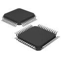
0 Uses0 StarsdsPIC33CK256MP205-I/M4
dsPIC dsPIC™ 33CK, Functional Safety (FuSa) Microcontroller IC 16-Bit 100MHz 256KB (256K x 8) FLASH 48-UQFN (6x6) 28/36/48/64/80-Pin Digital Signal Controllers with High-Resolution PWM and CAN Flexible Data (CAN FD) Operating Conditions • 3.0V to 3.6V, -40°C to +125°C, DC to 100 MIPS • 3.0V to 3.6V, -40°C to +150°C, DC to 70 MIPS Core: 16-Bit dsPIC33CK CPU • 32-256 Kbytes of Program Flash with ECC and 8-24K RAM • Fast 6-Cycle Divide • LiveUpdate • Code Efficient (C and Assembly) Architecture • 40-Bit Wide Accumulators • Single-Cycle (MAC/MPY) with Dual Data Fetch • Single-Cycle, Mixed-Sign MUL Plus Hardware Divide • 32-Bit Multiply Support • Four Sets of Interrupt Context Saving Registers which Include Accumulator and STATUS for Fast Interrupt Handling • Zero Overhead Looping • RAM Memory Built-In Self-Test (MBIST) Clock Management • Internal Oscillator • Programmable PLLs and Oscillator Clock Sources • Reference Clock Output • Fail-Safe Clock Monitor (FSCM) • Fast Wake-up and Start-up • Backup Internal Oscillator Power Management • Low-Power Management Modes (Sleep, Idle, Doze) • Integrated Power-on Reset and Brown-out Reset High-Speed PWM • Eight PWM Pairs • Up to 250 ps PWM Resolution • Dead Time for Rising and Falling Edges • Dead-Time Compensation • Clock Chopping for High-Frequency Operation • PWM Support for: - DC/DC, AC/DC, inverters, PFC, lighting - BLDC, PMSM, ACIM, SRM motors • Fault and Current Limit Inputs • Flexible Trigger Configuration for ADC Triggering Timers/Output Compare/Input Capture • One General Purpose Timer • Peripheral Trigger Generator (PTG): - Up to 15 trigger sources to other peripheral modules - CPU independent state machine-based instruction sequencer • Nine MCCP/SCCP modules which Include Timer, Capture/Compare and PWM: - One MCCP - Eight SCCPs - 16 or 32-bit time base - 16 or 32-bit capture - 4-deep capture buffer • Fully Asynchronous Operation, Available in Sleep Modes #CommonPartsLibrary #IntegratedCircuit #Microcontroller #DSPIC33CK256MP
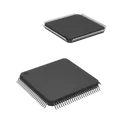
10 Uses0 StarsSTM32F407VGT6
ARM Microcontrollers - MCU ARM M4 1024 FLASH 168 Mhz 192kB SRAM 100-LQFP (14x14) Arm® Cortex®-M4 32b MCU+FPU, 210DMIPS, up to 1MB Flash/192+4KB RAM, USB OTG HS/FS, Ethernet, 17 TIMs, 3 ADCs, 15 comm. interfaces & camera • Core: Arm® 32-bit Cortex®-M4 CPU with FPU, Adaptive real-time accelerator (ART Accelerator) allowing 0-wait state execution from Flash memory, frequency up to 168 MHz, memory protection unit, 210 DMIPS/ 1.25 DMIPS/MHz (Dhrystone 2.1), and DSP instructions • Memories – Up to 1 Mbyte of Flash memory – Up to 192+4 Kbytes of SRAM including 64- Kbyte of CCM (core coupled memory) data RAM – 512 bytes of OTP memory – Flexible static memory controller supporting Compact Flash, SRAM, PSRAM, NOR and NAND memories • LCD parallel interface, 8080/6800 modes • Clock, reset and supply management – 1.8 V to 3.6 V application supply and I/Os – POR, PDR, PVD and BOR – 4-to-26 MHz crystal oscillator – Internal 16 MHz factory-trimmed RC (1% accuracy) – 32 kHz oscillator for RTC with calibration – Internal 32 kHz RC with calibration • Low-power operation – Sleep, Stop and Standby modes –VBAT supply for RTC, 20×32 bit backup registers + optional 4 KB backup SRAM • 3×12-bit, 2.4 MSPS A/D converters: up to 24 channels and 7.2 MSPS in triple interleaved mode • 2×12-bit D/A converters • General-purpose DMA: 16-stream DMA controller with FIFOs and burst support • Up to 17 timers: up to twelve 16-bit and two 32- bit timers up to 168 MHz, each with up to 4 IC/OC/PWM or pulse counter and quadrature (incremental) encoder input • Debug mode – Serial wire debug (SWD) & JTAG interfaces – Cortex-M4 Embedded Trace Macrocell™ • Up to 140 I/O ports with interrupt capability – Up to 136 fast I/Os up to 84 MHz – Up to 138 5 V-tolerant I/Os • Up to 15 communication interfaces – Up to 3 × I2C interfaces (SMBus/PMBus) – Up to 4 USARTs/2 UARTs (10.5 Mbit/s, ISO 7816 interface, LIN, IrDA, modem control) – Up to 3 SPIs (42 Mbits/s), 2 with muxed full-duplex I2S to achieve audio class accuracy via internal audio PLL or external clock – 2 × CAN interfaces (2.0B Active) – SDIO interface • Advanced connectivity – USB 2.0 full-speed device/host/OTG controller with on-chip PHY – USB 2.0 high-speed/full-speed device/host/OTG controller with dedicated DMA, on-chip full-speed PHY and ULPI – 10/100 Ethernet MAC with dedicated DMA: supports IEEE 1588v2 hardware, MII/RMII #CommonPartsLibrary #IntegratedCircuit #Microcontroller #STM32F407
62 Uses0 StarsSE868K3-A
Telit SE868K3-A/AL GNSS antenna module, multi-constellation GPS/QZSS/GLONASS receiver with Galileo ready support, integrated 9x9mm patch antenna, SAW filter, LNA, flash memory, RTC and TCXO, 11x11mm SMT PCB package, supports UART/I2C/SPI interfaces, A-GPS ephemeris prediction/injection, SBAS compliant, simultaneous GPS+GLONASS/Galileo tracking, optimized RF path, low power consumption, backward compatible with SE868-A series. SE868K3
15 Uses0 StarsMIMXRT1176DVMAA
ARM® Cortex®-M4, Cortex®-M7 RT1170 Microcontroller IC 32-Bit Dual-Core 400MHz, 800MHz External Program Memory 289-LFBGA (14x14) Pre-ordered MCUs MIMXRT1176DVMAA MAPBGA-289_L14.0-W14.0-R17-C17-P0.80-TL LCSC Part Number: C1020237 JLCPCB Part Class: Extended Part Manufactured by NXP(恩智浦)
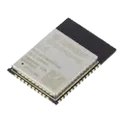
51 Uses0 StarsESP32-WROOM-32E (16MB)
The ESP32-WROOM-32E (16MB) is a highly integrated Wi-Fi + Bluetooth + Bluetooth Low Energy (BLE) module developed by Espressif. It is based on the ESP32-D0WD-V3 chip and features a dual-core processor, rich peripherals, and large flash memory—making it ideal for IoT, embedded systems, and wireless applications. This module is part of the upgraded WROOM-32E series, offering improved RF performance, better stability, and enhanced reliability compared to earlier versions like the 32D. Key Features (16MB Variant) Processor & Memory Dual-core Xtensa® 32-bit LX6 CPU, up to 240 MHz 520 KB SRAM + 448 KB ROM 16 MB SPI Flash (large storage for firmware/data) Optional variants with PSRAM for memory-intensive tasks Connectivity 2.4 GHz Wi-Fi (802.11 b/g/n) Bluetooth v4.2 (BR/EDR + BLE) Integrated PCB antenna (no external antenna needed) Peripherals & Interfaces Up to 26–38 GPIOs (depending on usage) Supports: UART, SPI, I2C, I2S PWM (LED & motor control) ADC, DAC Capacitive touch sensors SD/SDIO/MMC, CAN (TWAI) Electrical & Physical Operating voltage: 3.0V – 3.6V Operating temperature: –40°C to +85°C (industrial range) Compact size: 18 × 25.5 × 3.1 mm Typical Applications Smart home devices (lighting, appliances) IoT sensors and gateways Industrial automation systems Wearables and smart gadgets Audio/voice processing (thanks to dual-core + large flash) #module #ESP32 #16MB
114 Uses0 StarsADXL345TCCZ-EP
Accelerometer X, Y, Z Axis ±2g, 4g, 8g, 16g 0.05Hz ~ 1.6kHz 14-LGA (3x5) The ADXL345-EP is an extended performance version of the ADXL345, which is a small, thin, ultralow power, 3-axis accelerometer with high resolution (13-bit) measurement at up to ±16 g. Digital output data is formatted as 16-bit twos complement and is accessible through either a SPI (3- or 4-wire) or I2 C digital interface. The ADXL345-EP is well suited for extended temperature range industrial and aerospace equipment. It measures the static acceleration of gravity in tilt-sensing applications, as well as dynamic acceleration resulting from motion or shock. Its high resolution (3.9 mg/LSB) enables measurement of inclination changes less than 1.0°. Several special sensing functions are provided. Activity and inactivity sensing detect the presence or lack of motion by comparing the acceleration on any axis with user-set thresholds. Tap sensing detects single and double taps in any direction. Freefall sensing detects if the device is falling. These functions can be mapped individually to either of two interrupt output pins. An integrated memory management system with a 32-level first in, first out (FIFO) buffer can be used to store data to minimize host processor activity and lower overall system power consumption. Low power modes enable intelligent motion-based power management with threshold sensing and active acceleration measurement at extremely low power dissipation. The ADXL345-EP is supplied in a small, thin, 3 mm × 5 mm × 1 mm, 14-lead, enhanced plastic package. Ultralow power: as low as 23 µA in measurement mode and 0.1 µA in standby mode at VS = 2.5 V (typical) Power consumption scales automatically with bandwidth User-selectable resolution from 10 to 13 bits 4 mg/LSB scale factor in all g ranges 32-sample FIFO minimizes host processor load Single tap, double tap, and free-fall detection Activity/inactivity monitoring Supply voltage range: 2.0 V to 3.6 V I/O voltage range: 1.7 V to VS SPI (3- and 4-wire) and I2C digital interfaces Flexible interrupt modes mappable to either interrupt pin Measurement ranges selectable via serial command Bandwidth selectable via serial command 10,000 g shock survival Pb free/RoHS compliant #commonpartslibrary #integratedcircuit #accelerometer
7 Uses0 StarsADXL345BCCZ
Accelerometer X, Y, Z Axis ±2g, 4g, 8g, 16g 0.05Hz ~ 1.6kHz 14-LGA (3x5) The ADXL345 is a small, thin, ultralow power, 3-axis accelerometer with high resolution (13-bit) measurement at up to ±16 g. Digital output data is formatted as 16-bit twos complement and is accessible through either a SPI (3- or 4-wire) or I2C digital interface. The ADXL345 is well suited for mobile device applications. It measures the static acceleration of gravity in tilt-sensing applications, as well as dynamic acceleration resulting from motion or shock. Its high resolution (3.9 mg/LSB) enables measurement of inclination changes less than 1.0°. Several special sensing functions are provided. Activity and inactivity sensing detect the presence or lack of motion by comparing the acceleration on any axis with user-set thresholds. Tap sensing detects single and double taps in any direction. Free-fall sensing detects if the device is falling. These functions can be mapped individually to either of two interrupt output pins. An integrated memory management system with a 32-level first in, first out (FIFO) buffer can be used to store data to minimize host processor activity and lower overall system power consumption. Low power modes enable intelligent motion-based power management with threshold sensing and active acceleration measurement at extremely low power dissipation. The ADXL345 is supplied in a small, thin, 3 mm × 5 mm × 1 mm, 14-lead, plastic package. ► Ultralow power: as low as 23 µA in measurement mode and 0.1 µA in standby mode at VS = 2.5 V (typical) ► Power consumption scales automatically with bandwidth ► User-selectable resolution ► Fixed 10-bit resolution ► Full resolution, where resolution increases with g range, up to 13-bit resolution at ±16 g (maintaining 4 mg/LSB scale factor in all g ranges) ► Embedded memory management system with FIFO technology minimizes host processor load ► Single tap/double tap detection ► Activity/inactivity monitoring ► Free-fall detection ► Supply voltage range: 2.0 V to 3.6 V ► I/O voltage range: 1.7 V to VS ► SPI (3- and 4-wire) and I2C digital interfaces ► Flexible interrupt modes mappable to either interrupt pin ► Measurement ranges selectable via serial command ► Bandwidth selectable via serial command ► Wide temperature range (−40°C to +85°C) ► 10,000 g shock survival ► Pb free/RoHS compliant #CommonPartsLibrary #IntegratedCircuit #Sensor #Transducer #Motion-Sensor #Accelerometer #ADXL345
63 Uses0 StarsSTM32F103C8T6
ARM® Cortex® M3 STM32F1 Microcontroller IC 32-Bit Single-Core 72MHz 64KB (64K x 8) FLASH Medium-density performance line Arm®-based 32-bit MCU with 64 or 128 KB Flash, USB, CAN, 7 timers, 2 ADCs, 9 com. interfaces Arm® 32-bit Cortex®-M3 CPU core – 72 MHz maximum frequency, 1.25 DMIPS/MHz (Dhrystone 2.1) performance at 0 wait state memory access – Single-cycle multiplication and hardware division • Memories – 64 or 128 Kbytes of Flash memory – 20 Kbytes of SRAM • Clock, reset and supply management – 2.0 to 3.6 V application supply and I/Os – POR, PDR, and programmable voltage detector (PVD) – 4 to 16 MHz crystal oscillator – Internal 8 MHz factory-trimmed RC – Internal 40 kHz RC – PLL for CPU clock – 32 kHz oscillator for RTC with calibration • Low-power – Sleep, Stop and Standby modes – VBAT supply for RTC and backup registers • 2x 12-bit, 1 µs A/D converters (up to 16 channels) – Conversion range: 0 to 3.6 V – Dual-sample and hold capability – Temperature sensor • DMA – 7-channel DMA controller – Peripherals supported: timers, ADC, SPIs, I 2Cs and USARTs • Up to 80 fast I/O ports – 26/37/51/80 I/Os, all mappable on 16 external interrupt vectors and almost all 5 V-tolerant Debug mode: – Serial wire debug (SWD) and JTAG interfaces • Seven timers – Three 16-bit timers, each with up to 4 IC/OC/PWM or pulse counter and quadrature (incremental) encoder input – 16-bit, motor control PWM timer with dead-time generation and emergency stop – Two watchdog timers (independent and window) – SysTick timer 24-bit downcounter • Up to nine communication interfaces – Up to two I2C interfaces (SMBus/PMBus®) – Up to three USARTs (ISO 7816 interface, LIN, IrDA capability, modem control) – Up to two SPIs (18 Mbit/s) – CAN interface (2.0B Active) – USB 2.0 full-speed interface • CRC calculation unit, 96-bit unique ID • Packages are ECOPACK #commonpartslibrary #integratedcircuit #microcontroller #stm32f1
36 Uses0 Stars