Interface ICs
An interface IC is a type of integrated circuit that is designed to facilitate communication between two devices or systems. These devices are commonly used in electronic systems to enable the transfer of data and control signals between different components or subsystems. Some common use cases for interface ICs include connecting microcontrollers to peripherals such as sensors or displays, linking multiple processors together in a network, and enabling communication between devices using different communication protocols. Flux.ai has the world's largest community-driven public library of interface ICs, with footprints, symbols, datasheets, and simulation models. This library is a valuable resource for engineers and designers who need access to accurate and up-to-date information on these important components. Whether you are working on a new design project or simply looking to learn more about interface ICs, Flux.ai is an excellent resource to help you find the information you need.
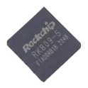
RK809-5
Rockchip RK809 highly integrated PMIC with audio codec for multi-core system applications, providing five configurable synchronous step-down converters, nine LDO regulators, two switches, battery fuel gauge, configurable power-up/power-down sequencing, integrated RTC with 32.768kHz clock support, I2C interface for voltage and fuel gauge control, dynamic DC/DC output voltage adjustment, soft-start on all channels, 2MHz switching frequency, integrated power switches, headphone driver and Class-D audio driver, QFN68 7.0 x 7.0mm package. Search Keywords: RK809, Rockchip RK809, RK809 PMIC, RK809 power management IC, RK809 codec PMIC, RK809 battery fuel gauge, RK809 audio codec, RK809 DC DC converter, RK809 LDO regulator, RK809 I2C PMIC, RK809 RTC, RK809 QFN68, Rockchip PMIC, RK809 datasheet Hashtags: #RK809 #RockchipRK809 #RockchipPMIC #PMIC #PowerManagementIC #AudioCodecPMIC #BatteryFuelGauge #DCDCConverter #LDORegulator #I2CPMIC #RTC #ClassDAudio #QFN68
3 Uses0 StarsRK809-5
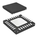
QFN-68-EP(7x7) Power Management - Specialized RoHS The RK809-5 is a highly integrated Power Management Integrated Circuit (PMIC) from Rockchip designed for multi-core processor systems and embedded applications. It provides a complete power management solution by integrating multiple high-efficiency DC-DC buck converters, LDO regulators, power sequencing logic, battery fuel gauging, RTC functionality, and audio codec capabilities into a single device. The RK809-5 is commonly used alongside Rockchip SoCs in single-board computers, tablets, AIoT devices, and industrial embedded systems. Key Features Five high-efficiency synchronous buck converters with fast transient response. Nine low-dropout (LDO) voltage regulators for powering sensitive analog and digital circuits. Integrated battery fuel gauge for battery capacity monitoring. Configurable power-up and power-down sequencing (OTP programmable). Dynamic Voltage Scaling (DVS/DVFS) support via I²C interface. Integrated Real-Time Clock (RTC) with 32.768 kHz crystal oscillator support. Two integrated load switches for peripheral power control. Over-current, over-voltage, and thermal protection features. Built-in audio CODEC with headphone driver and Class-D amplifier support. Designed to minimize external component count and simplify power system design. QFN-68-EP (7 mm × 7 mm) package. #RK8095 #RK809 #Rockchip #PMIC #PowerManagementIC #BatteryManagement #AudioCodec #RTC #DVFS #EmbeddedSystems #SingleBoardComputer #IoT #IndustrialElectronics #PowerSupplyDesign #ElectronicsEngineering
11 Uses0 StarsMT29F256G08AUCABH3-10ITZ:A
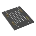
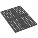
SLC NAND Flash Parallel/Serial 3.3V 256G-bit 32G x 8 100-Pin LBGA FLASH - NAND (SLC) Memory IC 256Gbit Parallel 100 MHz 100-LBGA (12x18) The MT29F256G08AUCABH3-10ITZ:A is a high-density 256Gb Single-Level Cell (SLC) NAND Flash memory device from Micron Technology. It provides non-volatile data storage with high reliability, fast read/write performance, and long endurance, making it suitable for industrial, networking, embedded computing, automotive, and data-logging applications. The device supports both asynchronous and synchronous interfaces and complies with the Open NAND Flash Interface (ONFI) standard for enhanced interoperability and performance. It is housed in a compact 100-ball LBGA package (12 mm × 18 mm). • Open NAND Flash Interface (ONFI) 2.2-compliant1 • Single-level cell (SLC) technology • Organization – Page size x8: 8640 bytes (8192 + 448 bytes) – Block size: 128 pages (1024K + 56K bytes) – Plane size: 2 planes x 2048 blocks per plane – Device size: 32Gb: 4096 blocks; 64Gb: 8192 blocks; 128Gb: 16,384 blocks; 256Gb: 32,768 blocks • Synchronous I/O performance – Up to synchronous timing mode 5 – Clock rate: 10ns (DDR) – Read/write throughput per pin: 200 MT/s • Asynchronous I/O performance – Up to asynchronous timing mode 5 – tRC/tWC: 20ns (MIN) – Read/write throughput per pin: 50 MT/s • Array performance – Read page: 35µs (MAX) – Program page: 350µs (TYP) – Erase block: 1.5ms (TYP) • Operating Voltage Range – VCC: 2.7–3.6V – VCCQ: 1.7–1.95V, 2.7–3.6V • Command set: ONFI NAND Flash Protocol • Advanced Command Set – Program cache – Read cache sequential – Read cache random – One-time programmable (OTP) mode – Multi-plane commands – Multi-LUN operations – Read unique ID – Copyback • First block (block address 00h) is valid when shipped from factory. For minimum required ECC, see Error Management (page 114). • RESET (FFh) required as first command after power-on • Operation status byte provides software method for detecting – Operation completion – Pass/fail condition – Write-protect status • Data strobe (DQS) signals provide a hardware method for synchronizing data DQ in the synchronous interface • Copyback operations supported within the plane from which data is read • Quality and reliability – Data retention: JESD47G compliant; see qualification report – Endurance: 60,000 PROGRAM/ERASE cycles • Operating temperature: – Commercial: 0°C to +70°C – Industrial (IT): –40ºC to +85ºC • Package – 52-pad LGA – 48-pin TSOP – 100-ball BGA – 132-ball BGA #Micron #NANDFlash #SLCNAND #FlashMemory #NonVolatileMemory #ONFI #EmbeddedSystems #IndustrialElectronics #DataStorage #MemoryIC #LBGA100 #HighReliability #MT29F256G08AUCABH310ITZA #MicronMemory #ParallelNANDFlash
3 Uses0 StarsATMEGA32U4-AU
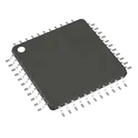
Microchip ATmega32U4 high-performance low-power 8-bit AVR microcontroller with integrated USB 2.0 full-speed device controller, up to 16MHz operation, 32KB Flash memory, 2.5KB SRAM and 1KB EEPROM, 12-channel 10-bit ADC, timers, PWM, SPI, TWI/I2C, USART, JTAG debug interface, watchdog timer, brown-out detection and multiple sleep modes, operating voltage range 2.7V to 5.5V, available in TQFP-44 and QFN-44 packages. Search Keywords: ATmega32U4, Microchip ATmega32U4, Atmel ATmega32U4, AVR USB microcontroller, 8-bit AVR MCU, ATmega32U4 USB, ATmega32U4 TQFP44, ATmega32U4 QFN44, 32KB Flash AVR, Arduino Leonardo MCU, Pro Micro MCU, ATmega32U4 datasheet Hashtags: #ATmega32U4 #MicrochipATmega32U4 #AtmelATmega32U4 #AVRMicrocontroller #8bitMCU #USBMicrocontroller #USBFullSpeed #32KBFlash #ArduinoLeonardoMCU #ProMicroMCU #TQFP44 #QFN44MCU AVR 32K FLASH 16MHZ 44-TQFP Atmel ATMEGA32U4-AU, 8bit AVR Microcontroller, 16MHz, 1 kB, 32 kB Flash, 44-Pin TQFP USB-C Pro Micro ATmega32U4 / Elite-C compatible module
23 Uses0 StarsSTSAFE-A110SO8
STMicroelectronics STSAFE-A110 secure element IC for authentication and secure data management, designed for IoT devices, smart home, smart city, industrial applications, consumer electronics and accessories. Supports authentication to remote or local hosts, secure channel establishment with TLS handshake support, secure boot and firmware upgrade signature verification, host pairing, secure counters, local host envelope wrapping/unwrapping, symmetric data encryption/decryption, on-chip key pair generation, LPWAN security support, ECC cryptography with NIST P-256/P-384, ECDSA, ECDH, SHA-256/SHA-384, 6KB configurable EEPROM, I2C interface, 1.62V to 5.5V supply voltage, -40°C to +105°C operating temperature, available in SO8N and UFDFPN8 packages. Search Keywords: STSAFE-A110, STSAFEA110, STMicroelectronics STSAFE-A110, STSAFE secure element, secure element IC, IoT authentication IC, hardware security IC, secure authentication chip, I2C secure element, ECC secure element, ECDSA ECDH secure chip, TLS authentication IC, secure boot authentication, firmware upgrade security IC, LPWAN security chip, SO8N secure element, UFDFPN8 secure element Hashtags: #STSAFEA110 #STSAFE #STMicroelectronics #SecureElement #AuthenticationIC #IoTSecurity #HardwareSecurity #SecureBoot #FirmwareAuthentication #ECCSecurity #ECDSA #ECDH #TLSHandshake #I2CSecurity #LPWANSecurity #SO8N #UFDFPN8STMicroelectronics Authentication, state-of-the-art security for peripherals and IoT devices
0 Uses0 StarsADS1293CISQ/NOPB
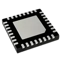
3 Channel AFE 24 Bit 28-WQFN (5x5) ADS1293CISQ/NOPB is a highly integrated, low-power 3-channel ECG Analog Front-End (AFE) from Texas Instruments. It is designed for portable and battery-powered medical devices, fitness monitors, heart-rate monitoring systems, Holter monitors, and other electrocardiogram (ECG) applications. The device integrates signal acquisition, filtering, lead-off detection, right-leg drive generation, and high-resolution analog-to-digital conversion into a single IC, reducing external component count and system cost. Key Features Three high-resolution ECG acquisition channels 24-bit analog-to-digital conversion Simultaneous pace detection support Ultra-low power consumption of approximately 0.3 mW per channel Low input-referred noise of 7 µVpp (40 Hz bandwidth) Programmable sample rates up to 25.6 ksps Differential input voltage range of ±400 mV Integrated EMI-hardened input filters Flexible input routing matrix Built-in Right-Leg Drive (RLD) amplifier AC and DC lead-off detection Integrated Wilson and Goldberger terminal generation Battery voltage monitoring capability Internal oscillator and voltage reference ALARMB pin for interrupt-driven diagnostics and fault reporting Multiple power-down and standby modes for battery-powered systems SPI-compatible digital interface Operating temperature range: –20°C to +85°C 28-pin WQFN package (5 mm × 5 mm) Typical Applications Portable 1-, 3-, 5-, 6-, 7-, 8-, and 12-lead ECG systems Holter monitors Event recorders Telemedicine devices Patient vital-sign monitoring equipment Automated External Defibrillators (AEDs) Sports and fitness heart-rate monitors Wearable medical devices Hashtags #commonpartslibrary #integratedcircuit #TexasInstruments #ADS1293 #AFE #AnalogFrontEnd #ECG #Electrocardiogram #MedicalElectronics #HealthTech #WearableDevices #HeartRateMonitor #PatientMonitoring #BiomedicalEngineering #24BitADC #LowPowerDesign #SPI #SignalConditioning #PortableMedicalDevices #HolterMonitor #Telemedicine #VitalSignsMonitoring #EmbeddedSystems #MixedSignalIC #WQFN28 #BatteryPoweredDevices #MedicalInstrumentation
3 Uses0 StarsPCA9450CHNY
Power Management IC for iMX8M 5V 6A 6 Buck + 5 LDO The PCA9450CHNY is a highly integrated Power Management Integrated Circuit (PMIC) from NXP Semiconductors, specifically designed to power the i.MX 8M family of application processors, particularly the i.MX 8M Plus. It integrates multiple high-efficiency DC-DC buck converters, LDO regulators, power sequencing logic, load switching, voltage monitoring, and system control functions into a single device. The PCA9450C variant features a configurable dual-phase 6 A buck regulator for powering high-current processor cores while supporting Dynamic Voltage Scaling (DVS) for optimized power efficiency. Key Features Six high-efficiency switching regulators (Buck converters) PCA9450C variant supports a configurable 6 A dual-phase buck regulator Three 3 A buck regulators with Dynamic Voltage Scaling (DVS) Remote-sense capability on major buck outputs for IR-drop compensation Five integrated LDO regulators Supports DDR4, LPDDR4, and DDR3L memory configurations 400 mA load switch with active discharge Dual-channel logic level translator Integrated 32.768 kHz crystal oscillator driver Fast-mode Plus (Fm+) 1 MHz I²C interface Programmable power sequencing and voltage control Power ON/OFF and Standby/Run mode control inputs Protection features including UVLO, thermal shutdown, fault monitoring, and soft-start Operating temperature range: −40°C to +105°C 56-pin HVQFN package (7 mm × 7 mm, 0.4 mm pitch) Optimized for i.MX 8M Mini, Nano, and Plus processors, especially the i.MX 8M Plus for the PCA9450C variant. #CommonPartsLibrary #PCA9450CHNY #PCA9450C #NXP #PMIC #PowerManagementIC #PowerSupply #VoltageRegulator #BuckConverter #LDO #DynamicVoltageScaling #DVS #IMX8M #IMX8MPlus #EmbeddedSystems #IndustrialElectronics #PowerManagement #HVQFN56 #Semiconductor #IntegratedCircuit #IC #CommonPartsLibrary #ElectronicsDesign #HardwareDesign #PCBDesign #EmbeddedLinux #IoT #ProcessorPowerManagement #PowerSequencing #SystemPower #NXPSemiconductors
12 Uses0 StarsMT53E1536M32D4DT-046 WT:A
SDRAM - Mobile LPDDR4 Memory IC 48Gbit 2.133 GHz MT53E1536M32D4DT-046 WT:A is a high-density 48Gb (6GB) LPDDR4/LPDDR4X SDRAM memory device from Micron Technology. It is designed for high-performance, low-power applications requiring fast memory bandwidth and efficient power management. The device features a 32-bit data bus, supports data rates up to 4266 MT/s, and is packaged in a compact 200-ball FBGA, making it suitable for embedded computing, industrial systems, networking equipment, AI edge devices, automotive electronics, and mobile platforms. Key Features 48Gb (6GB) LPDDR4/LPDDR4X SDRAM Organized as 1.5G × 32 bits Data transfer rates up to 4266 MT/s Maximum clock frequency of 2133 MHz Low-power operation with 1.1V core supply 32-bit memory interface 200-ball FBGA package JEDEC LPDDR4-compliant architecture Per-bank refresh support Temperature-compensated refresh Self-refresh and deep power-down modes Partial-array self-refresh capability High bandwidth with reduced power consumption Optimized for compact embedded designs Operating temperature range: –30°C to +85°C Typical Applications Embedded Linux computers Single-board computers (SBCs) AI and edge computing platforms Industrial automation systems Networking and telecommunications equipment Automotive infotainment and control systems Tablets and mobile devices FPGA and SoC-based designs #commonpartslibrary #integratedcircuit #memory #dram #sdram #lpddr4 #lpddr4x #mobiledram #micron #embeddedsystems #embeddedcomputing #industrialelectronics #automotiveelectronics #edgecomputing #artificialintelligence #networking #telecommunications #highspeedmemory #lowpowerdesign #computerhardware #electroniccomponents #semiconductor #datasheet #fbga #memorychip #electronicsdesign #pcbdesign #hardwareengineering #electronicengineering #systemonchip #fpga #iot #internetofthings #computermemory #digitalelectronics #surfaceMount #smt #bga #storage #highperformancecomputing #hpc #mobiledevices #industrialautomation #electronicdesign #componentlibrary #fluxlibrary #parametricpart #eda #schematic #pcb #electronicdesignautomation #chipdesign #embeddedhardware #memorymodule #lowpowerelectronics #highbandwidthmemory #electronics #hardwaredevelopment #engineering #electricalengineering
1 Uses0 StarsSTM32L432KCU6
ST Microelectronics STM32L432KCU6 UFQFPN-32_L5.0-W5.0-P0.50-TL-EP3.5 LCSC Part Number: C1337280 JLCPCB Part Class: Extended Part Manufactured by ST(意法半导体) STMicroelectronics STM32L432KC ultra-low-power 32-bit ARM Cortex-M4 microcontroller with FPU running up to 80MHz, featuring 256KB Flash memory, 64KB SRAM, USB 2.0 Full-Speed device support, Quad-SPI interface, RTC with calendar and alarms, true random number generator (TRNG), DMA controller, CAN 2.0B, UART, LPUART, SPI, I2C, SAI audio interface, 12-bit 5MSPS ADC, dual 12-bit DACs, operational amplifier with PGA, comparators, capacitive sensing channels, advanced timers and ultra-low-power modes. Operates from 1.71V to 3.6V and is optimized for battery-powered, industrial, medical, IoT and portable embedded applications. Search Keywords: STM32L432KC, STM32L432KCU6, STM32L432KCU6TR, STM32L432, STM32L4 series, STM32 Cortex-M4 MCU, STM32 low power microcontroller, STM32 256KB Flash 64KB SRAM, STM32 USB FS MCU, STM32 CAN MCU, STM32 Quad SPI MCU, STM32L432 datasheet, STM32L432 development board, Nucleo-L432KC, ARM Cortex-M4 FPU Hashtags: #STM32L432KC #STM32L432KCU6 #STM32L432 #STM32L4 #STMicroelectronics #CortexM4 #ARMMicrocontroller #LowPowerMCU #EmbeddedSystems #USBFS #CANBus #QuadSPI #ADC12bit #DAC12bit #RTC #TRNG #IoTMCU #IndustrialMCU #MedicalElectronics #NucleoL432KC
46 Uses0 StarsADF4351BCPZ
Clock Generators, PLLs, Frequency Synthesizers ADF4351BCPZ LFCSP-32_L5.0-W5.0-P0.50-BL-EP3.5 LCSC Part Number: C654681 JLCPCB Part Class: Extended Part Manufactured by ADI(亚德诺)/LINEAR(凌特) Analog Devices ADF4351 wideband fractional-N and integer-N PLL frequency synthesizer with integrated voltage-controlled oscillator (VCO), generating RF output frequencies from 35MHz to 4.4GHz. Features low phase noise, programmable output divider ratios (/1, /2, /4, /8, /16, /32, /64), programmable RF output power, dual-modulus prescaler (4/5 or 8/9), analog and digital lock detect, fast lock mode, cycle slip reduction, auxiliary RF output, RF mute function, and 3-wire serial programming interface. Operates from 3.0V to 3.6V and is widely used in RF signal generators, local oscillators, SDR systems, wireless infrastructure, test equipment, microwave communications, clock generation, and laboratory instrumentation. Search Keywords: ADF4351, Analog Devices ADF4351, ADF4351BRUZ, RF synthesizer, PLL synthesizer, fractional N PLL, integer N PLL, integrated VCO, 35MHz to 4.4GHz synthesizer, RF signal generator IC, microwave frequency synthesizer, local oscillator PLL, SDR synthesizer, programmable RF generator, low phase noise synthesizer, SPI PLL synthesizer, RF clock generator Hashtags: #ADF4351 #AnalogDevices #PLL #FractionalNPLL #IntegerNPLL #FrequencySynthesizer #RFSynthesizer #IntegratedVCO #RFGenerator #SignalGenerator #LocalOscillator #MicrowaveRF #SDR #ClockGenerator #RFIC #WirelessInfrastructure #TestEquipment #LowPhaseNoise #SPIInterface #ADF4351Module
43 Uses0 Stars