Interface ICs
An interface IC is a type of integrated circuit that is designed to facilitate communication between two devices or systems. These devices are commonly used in electronic systems to enable the transfer of data and control signals between different components or subsystems. Some common use cases for interface ICs include connecting microcontrollers to peripherals such as sensors or displays, linking multiple processors together in a network, and enabling communication between devices using different communication protocols. Flux.ai has the world's largest community-driven public library of interface ICs, with footprints, symbols, datasheets, and simulation models. This library is a valuable resource for engineers and designers who need access to accurate and up-to-date information on these important components. Whether you are working on a new design project or simply looking to learn more about interface ICs, Flux.ai is an excellent resource to help you find the information you need.
SN65HVD75D
1/1 Transceiver Half RS422, RS485 8-SOIC These devices have robust 3.3-V drivers and receivers in a small package for demanding industrial applications. The bus pins are robust to ESD events with high levels of protection to Human-Body Model and IEC Contact Discharge specifications. Each of these devices combines a differential driver and a differential receiver which operate from a single 3.3-V power supply. The driver differential outputs and the receiver differential inputs are connected internally to form a bus port suitable for half-duplex (two-wire bus) communication. These devices feature a wide common-mode voltage range making the devices suitable for multi-point applications over long cable runs. These devices are characterized from –40°C to 125°C 1• Small-size VSSOP Packages Save Board Space, or SOIC for Drop-in Compatibility • Bus I/O Protection – >±15 kV HBM Protection – >±12 kV IEC 61000-4-2 Contact Discharge – >±4 kV IEC 61000-4-4 Fast Transient Burst • Extended Industrial Temperature Range –40°C to 125°C • Large Receiver Hysteresis (80 mV) for Noise Rejection • Low Unit-Loading Allows Over 200 Connected Nodes • Low Power Consumption – Low Standby Supply Current: < 2 µA – ICC < 1 mA Quiescent During Operation • 5-V Tolerant Logic Inputs Compatible With 3.3-V or 5-V Controllers • Signaling Rate Options Optimized for: 250 kbps, 20 Mbps, 50 Mbps • Glitch Free Power-Up and Power-Down Bus Inputs and Outputs 2 Applications • Factory Automation • Telecommunications Infrastructure • Motion Control #SN65HVD75D #RS485 #RS422 #Transceiver #TexasInstruments #IndustrialCommunication #FactoryAutomation #MotionControl #TelecomInfrastructure #ESDProtection #HalfDuplex #InterfaceIC #EmbeddedSystems #IndustrialElectronics #DataCommunication
146 Uses0 StarsAD74413RBCPZ
Analog Devices AD74413R is a quad-channel software-configurable analog and digital input/output (I/O) controller designed for industrial automation, process control, building management, and smart sensing systems. Each channel can be independently configured as voltage input, current input, voltage output, current output, digital input, RTD temperature measurement, or thermocouple interface, enabling highly flexible universal I/O architectures. The device integrates four 16-bit sigma-delta ADCs, four 13-bit DACs, precision voltage references, diagnostics, open-circuit and short-circuit detection, internal temperature monitoring, and HART communication support. Communication with the host processor is performed through an SPI interface. The AD74413R simplifies PLC, DCS, remote I/O, industrial sensor, actuator, and process instrumentation designs by replacing multiple dedicated analog front-end components with a single programmable I/O solution. Search Keywords: AD74413R, Analog Devices universal I/O, software configurable I/O, industrial I/O controller, analog input output IC, programmable PLC I/O, process control interface, RTD measurement IC, thermocouple interface IC, HART compatible I/O, SPI industrial interface, voltage input output controller, current loop controller, universal analog front end, remote I/O module IC, industrial automation controller AD74413R Hashtags: #AD74413R #AnalogDevices #UniversalIO #IndustrialAutomation #ProcessControl #PLC #RemoteIO #HART #RTD #Thermocouple #AnalogInput #AnalogOutput #CurrentLoop #IndustrialElectronics #SPIInterface #DAC #ADC #BuildingAutomation #Instrumentation #ElectronicComponentsQuad-Channel, Software Configurable Input and Output
5 Uses0 StarsW25Q128JVSIM
FLASH - NOR Memory IC 128Mb (16M x 8) SPI - Quad I/O, QPI, DTR 133 MHz 8-SOIC 128M-bit Serial Flash Memory with uniform 4KB sectors and Dual/Quad SPI Winbond W25Q128JV is a 128-Mbit (16 MB) serial NOR Flash memory device designed for code and data storage in embedded systems. It supports standard SPI, Dual SPI, Quad SPI (QSPI), and Dual/Quad Peripheral Interface (DPI/QPI) modes, enabling high-speed data transfer rates up to 133 MHz clock operation and up to 532 MB/s equivalent throughput in Quad I/O DTR mode. The device supports Execute-In-Place (XIP), allowing processors and microcontrollers to run code directly from external flash memory without copying it to RAM. Features include 4 KB sector erase, 32 KB and 64 KB block erase, page programming, hardware/software write protection, security registers, JEDEC identification, SFDP support, suspend/resume operations, and low-power standby modes. Suitable for microcontrollers, FPGA configuration storage, IoT devices, industrial controllers, networking equipment, consumer electronics, and embedded systems requiring reliable non-volatile memory. Search Keywords: W25Q128JV, Winbond flash memory, SPI NOR Flash, QSPI Flash, Quad SPI memory, Serial Flash memory, 128Mbit Flash, 16MB Flash memory, Execute In Place XIP, external MCU flash, ESP32 flash memory, FPGA configuration memory, NOR flash storage, W25Q128, Dual SPI Flash, Quad I/O Flash, embedded nonvolatile memory, serial flash IC Hashtags: #W25Q128JV #Winbond #NORFlash #SPIMemory #QSPI #SerialFlash #FlashMemory #EmbeddedSystems #Microcontroller #ESP32 #FPGA #NonVolatileMemory #XIP #IoT #ElectronicsDesign #MemoryIC #FirmwareStorage #QuadSPI #EmbeddedHardware #ElectronicComponents
83 Uses0 StarsW55RP20
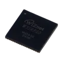
Ethernet ICs W55RP20 microcontroller, Dual ARM Cortex-M0+ a. 133MHz, 2MByte Flash memory on-chip, 264kB on-chip SRAM in six independent banks, DMA controller W55RP20 is a highly integrated System-in-Package (SiP) from WIZnet that combines the popular RP2040 dual-core microcontroller with a W5500 hardware TCP/IP Ethernet controller. Designed for IoT, industrial automation, and embedded networking applications, the W55RP20 delivers reliable Ethernet connectivity, low power consumption, and high-performance processing in a compact package. It simplifies Ethernet-enabled designs by integrating the MCU, network stack, flash memory, and Ethernet functionality into a single device. Key Features Dual-core ARM Cortex-M0+ processor running up to 133 MHz Integrated hardwired TCP/IP stack for reliable Ethernet communication 2 MB on-chip Flash memory 264 KB SRAM in six independent memory banks Built-in 10BASE-T / 100BASE-TX Ethernet MAC and PHY Supports TCP, UDP, IPv4, ICMP, ARP, IGMP, and PPPoE protocols 23 GPIO pins, including 4 analog-capable inputs 2× UART, 2× SPI, and 2× I²C interfaces 16 PWM channels and 8 Programmable I/O (PIO) state machines USB 1.1 Host/Device controller with integrated PHY 12-channel DMA controller for efficient data transfer Operating voltage range of 1.8 V to 3.3 V Industrial temperature support up to -40°C to +85°C Compact 68-QFN package for space-constrained designs #W55RP20 #WIZnet #RP2040 #EthernetMCU #IoT #EmbeddedSystems #IndustrialAutomation #TCPIP #EthernetController #Microcontroller #HardwareTCPIP #Networking #EmbeddedDesign #SmartDevices #IoTDevelopment
4 Uses0 StarsNRF54L15-CAAA-R7
IC RF TxRx + MCU 802.15.4, Bluetooth Bluetooth v5.4, Matter, Thread, Zigbee® 47-XFBGA, WLCSP # NRF54L15-CAAA-R7 ## General Description The NRF54L15-CAAA-R7 is an ultra-low-power wireless System-on-Chip (SoC) developed by [Nordic Semiconductor](https://www.nordicsemi.com?utm_source=chatgpt.com) for advanced Internet of Things (IoT), industrial, medical, smart home, and wireless sensing applications. The device integrates a high-performance Arm Cortex-M33 processor, a dedicated RISC-V coprocessor, large embedded memory resources, and a multiprotocol 2.4 GHz radio subsystem into a compact package. It is designed to provide exceptional energy efficiency, robust wireless connectivity, and enhanced security while supporting modern wireless standards including Bluetooth® Low Energy, Matter, Thread, Zigbee®, Bluetooth Mesh, Amazon Sidewalk, and proprietary 2.4 GHz protocols. The device is optimized for battery-powered applications requiring extended operating life, high processing capability, and scalable connectivity solutions. ## Key Features ### Processing Architecture * 128 MHz Arm® Cortex®-M33 application processor * Integrated 128 MHz RISC-V coprocessor * TrustZone® security architecture ### Memory Resources * 1.5 MB Non-Volatile Memory (NVM) * 256 KB RAM ### Wireless Connectivity * Multiprotocol 2.4 GHz RF transceiver * Bluetooth® Low Energy support * Matter support * Thread support * Zigbee® support * Bluetooth Mesh support * Amazon Sidewalk support * Proprietary 2.4 GHz protocol support * Bluetooth Channel Sounding capability * Compatible with Wi-Fi companion devices ### RF Performance * Data rates up to 4 Mbps * Output power up to +8 dBm * High receiver sensitivity for extended wireless range ### Security Features * Hardware cryptographic engine * Side-channel attack protection * Tamper detection mechanisms * Secure boot and secure firmware update support ### Peripheral Interfaces * SPI * I²C (TWI) * UART * I²S * GPIO * ADC * PWM * PDM * NFC * QDEC ### Power Characteristics * Ultra-low-power operation * Optimized sleep modes * Battery-powered application support * Operating supply voltage from 1.7 V to 3.6 V ### Package Information * WLCSP package * Surface-mount technology * Industrial operating temperature support ## Applications * Smart Home Devices * Industrial IoT Systems * Wearable Electronics * Medical and Healthcare Devices * Asset Tracking Solutions * Wireless Sensors * Building Automation Systems * Smart Lighting Controls * Consumer Electronics * Connected Peripheral Devices #NordicSemiconductor #nRF54L15 #NRF54L15CAAAR7 #BluetoothLE #Matter #Thread #Zigbee #IoT #WirelessSoC #EmbeddedSystems #IndustrialIoT #SmartHome #LowPowerDesign #CortexM33 #RISCV
11 Uses0 StarsSTM32MP157CAC3
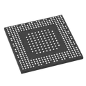
ARM® Cortex®-A7 Microprocessor IC STM32MP1 2 Core, 32-Bit 209MHz, 650MHz 361-TFBGA (12x12) # Engineering Specification ## Product Name STM32MP157CAC3 ## General Description STM32MP157CAC3 is a high-performance microprocessor unit that combines application processing and real-time control capabilities within a single integrated circuit. The device is designed to support advanced embedded systems requiring a balance of computing performance, deterministic control, multimedia processing, connectivity, and security functionality. The component integrates multi-core processing resources, memory interfaces, graphics capabilities, peripheral controllers, and communication subsystems to enable the development of sophisticated embedded platforms. Its heterogeneous architecture allows high-level operating systems and real-time firmware to operate simultaneously, supporting applications that require both user-interface functionality and low-latency control. The device is intended for industrial automation, human-machine interface systems, edge computing platforms, communication equipment, medical devices, smart infrastructure, and Internet of Things applications. Its architecture enables consolidation of system functions, reducing component count and simplifying overall hardware design. The design emphasizes processing efficiency, system scalability, power management, security, and long-term reliability. It supports advanced software ecosystems and facilitates the development of connected embedded products with graphical interfaces, networking capabilities, and real-time operational control. ## Functional Requirements ### Application Processing The device shall provide application-level processing capabilities suitable for operating systems, middleware, and user applications. ### Real-Time Processing The device shall support deterministic control functions for time-critical embedded operations. ### Multimedia Support The component shall support graphical and multimedia processing functions for display and user-interface applications. ### System Integration The device shall integrate processing, communication, and peripheral functions within a unified embedded computing platform. ## Electrical Requirements ### Power Management The device shall support efficient power operation and multiple power management modes to optimize energy consumption. ### Memory Interface Support The component shall support external memory devices for program execution, data storage, and system operation. ### Peripheral Connectivity The device shall provide interfaces for communication, control, monitoring, and external subsystem integration. ### Signal Integrity The design shall support reliable operation across supported interface standards and operating conditions. ## Processing Architecture Requirements ### Multi-Core Operation The device shall support concurrent execution of application and real-time workloads through integrated processing resources. ### Operating System Support The architecture shall support embedded operating systems and software frameworks suitable for advanced application development. ### Security Features The device shall support hardware-based mechanisms intended to protect system integrity, software assets, and sensitive data. ### Resource Management The component shall support efficient allocation of processing, memory, and peripheral resources. ## Mechanical Requirements ### Surface Mount Construction The device shall be supplied in a high-density surface mount package suitable for automated manufacturing processes. ### PCB Integration The package shall support integration into multilayer printed circuit boards designed for high-performance embedded systems. ### Structural Integrity The device shall maintain electrical and mechanical reliability during assembly and operational service life. ## Environmental Requirements ### Operating Conditions The component shall operate reliably within environmental conditions commonly encountered in industrial and embedded applications. ### Thermal Performance The device shall support stable operation under sustained processing workloads and associated thermal conditions. ### Storage and Handling The component shall maintain physical and electrical integrity during transportation, storage, and manufacturing processes. ## Quality Requirements ### Reliability The device shall provide dependable long-term operation in embedded and industrial computing environments. ### Verification Processing, peripheral, communication, and system functions shall be validated through applicable testing and qualification procedures. ### Compliance The product shall conform to relevant semiconductor, quality, and embedded computing standards applicable to its intended use. ## Documentation Requirements Technical documentation shall include processor architecture information, hardware integration guidelines, memory interface recommendations, power management considerations, software development support, security features, and application design guidance. ## Classification Tags #STM32MP157CAC3 #STM32MP1 #Microprocessor #MPU #EmbeddedProcessor #ARMProcessor #EmbeddedLinux #RealTimeControl #IndustrialAutomation #HumanMachineInterface #EdgeComputing #IoTGateway #EmbeddedSystems #SystemOnChip #SoC #ApplicationProcessor #GraphicsProcessor #ConnectivityPlatform #IndustrialElectronics #PCBDesign #HardwareDevelopment #ElectricalEngineering #CommonPartsLibrary #ComponentLibrary #EngineeringSpecification #TechnicalDocumentation #SystemIntegration #SecureEmbeddedSystems #MulticoreProcessing
9 Uses0 StarsLR2021IMLTRT
IC RF TxRx Only General ISM > 1GHz LoRaWAN 32-VFQFN Exposed Pad LR2021IMLTRT is a fourth-generation, long-range, low-power, multi-band LoRa® RF transceiver from Semtech, designed for IoT, LPWAN, satellite communication, smart metering, industrial automation, asset tracking, and wireless sensor networks. It supports operation across sub-GHz and 2.4 GHz frequency bands, offering excellent receiver sensitivity, high transmit power, and compatibility with multiple wireless protocols including LoRaWAN®, Bluetooth® LE PHY, Zigbee™, Thread®, Amazon Sidewalk, and Wi-SUN. Key Features Multi-band operation: 150 MHz to 960 MHz and 1.5 GHz to 2.5 GHz Supports LoRa®, LoRaWAN®, LR-FHSS, FLRC, FSK, GFSK, GMSK, MSK, OOK, and O-QPSK Maximum data rate up to 2.6 Mbps High receiver sensitivity up to -141.5 dBm (LoRa mode) Transmit power up to +22 dBm (sub-GHz) Compatible with Bluetooth® LE 5.0 PHY, Thread®, Zigbee™, Amazon Sidewalk, Sigfox, Wi-SUN, and Z-Wave® Ultra-low power consumption with 470 nA sleep current Operating voltage range: 1.8 V to 3.7 V SPI interface with programmable GPIOs Operating temperature range: -40°C to +85°C Compact 32-pin QFN (5 mm × 5 mm) package for space-constrained designs. Hashtags #Semtech #LR2021IMLTRT #LoRa #LoRaWAN #RFTransceiver #WirelessCommunication #IoT #LPWAN #BluetoothLE #Zigbee #Thread #WiSUN #AmazonSidewalk #AssetTracking #SmartMetering #IndustrialIoT #SatelliteCommunication #LowPowerDesign #EmbeddedSystems #RFIC
22 Uses0 Stars2286550-1
2286550-1 is a TE Connectivity Automotive HSD (High-Speed Data) hybrid connector header designed for high-speed data transmission in automotive applications. It is a shielded, right-angle PCB-mounted connector that combines HSD and MQS contacts, making it suitable for Ethernet, LVDS, USB, camera, infotainment, and other vehicle data communication systems. The connector features a 100 Ω controlled impedance design for reliable signal integrity in demanding automotive environments. Key Features Automotive HSD+2MQS hybrid header connector 6-position interface with A-coding Right-angle (horizontal) PCB mounting Board-to-board and wire-to-board connectivity Shielded construction for EMI protection 100 Ω impedance for high-speed data transmission Through-hole solder termination Operating voltage up to 60 VDC Maximum current rating: 2.5 A Operating frequency range: 0 to 3 GHz Gold-plated signal contacts for reliable performance Operating temperature range: -40°C to +105°C Reflow soldering capable Designed for automotive signal applications #CommonPartsLibrary #Connector #TEConnectivity #AutomotiveConnector #HSDConnector #DataConnectivity #HighSpeedData #AutomotiveEthernet #WireToBoard #BoardToBoard #ShieldedConnector #PCBConnector #AutomotiveElectronics #22865501
1 Uses0 StarsZ84C2006PEG
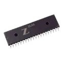
Interface - Specialized Z84C2006PEG PDIP-40_L52.3-W13.8-P2.54-LS15.2-BL LCSC Part Number: C2614542 JLCPCB Part Class: Extended Part Manufactured by Zilog Z84C00 / Z84C0008PEC PDIP-40 Zilog Z80 microprocessor family, fourth-generation enhanced 8-bit CPU architecture with high computational performance and efficient memory utilization. Features two complete sets of general-purpose registers (main and alternate register banks) for fast context switching, two 16-bit index registers (IX and IY), stack pointer, program counter, refresh register, and interrupt register. Supports a single +5V power supply and interfaces directly with standard memory and peripheral devices. Includes advanced interrupt handling, daisy-chain interrupt capability, and built-in dynamic RAM refresh support. Widely used in industrial control systems, embedded equipment, terminals, instrumentation, retro computers, and communication devices. Search Keywords: Z80 CPU, Zilog Z80, Z84C00, Z8400, 8-bit microprocessor, enhanced Z80 processor, DIP40 CPU, CMOS Z80, NMOS Z80, embedded processor, industrial controller CPU, retro computer processor, vintage microprocessor, dynamic RAM refresh CPU, interrupt controller compatible CPU Hashtags: #Z80 #Zilog #Z84C00 #Z8400 #8BitCPU #Microprocessor #EmbeddedSystems #IndustrialElectronics #RetroComputing #VintageComputing #DIP40 #ComputerArchitecture #DigitalElectronics #CPU #ClassicComputing
0 Uses0 StarsZ84C0006PEG
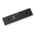
Zilog Z80 microprocessor family, fourth-generation enhanced 8-bit CPU architecture with high computational performance and efficient memory utilization. Features two complete sets of general-purpose registers (main and alternate register banks) for fast context switching, two 16-bit index registers (IX and IY), stack pointer, program counter, refresh register, and interrupt register. Supports a single +5V power supply and interfaces directly with standard memory and peripheral devices. Includes advanced interrupt handling, daisy-chain interrupt capability, and built-in dynamic RAM refresh support. Widely used in industrial control systems, embedded equipment, terminals, instrumentation, retro computers, and communication devices. Search Keywords: Z80 CPU, Zilog Z80, Z84C00, Z8400, 8-bit microprocessor, enhanced Z80 processor, DIP40 CPU, CMOS Z80, NMOS Z80, embedded processor, industrial controller CPU, retro computer processor, vintage microprocessor, dynamic RAM refresh CPU, interrupt controller compatible CPU Hashtags: #Z80 #Zilog #Z84C00 #Z8400 #8BitCPU #Microprocessor #EmbeddedSystems #IndustrialElectronics #RetroComputing #VintageComputing #DIP40 #ComputerArchitecture #DigitalElectronics #CPU #ClassicComputingMicroprocessors - MPU 6MHz Z80 CMOS CPU XT
3 Uses0 Stars