Interface ICs
An interface IC is a type of integrated circuit that is designed to facilitate communication between two devices or systems. These devices are commonly used in electronic systems to enable the transfer of data and control signals between different components or subsystems. Some common use cases for interface ICs include connecting microcontrollers to peripherals such as sensors or displays, linking multiple processors together in a network, and enabling communication between devices using different communication protocols. Flux.ai has the world's largest community-driven public library of interface ICs, with footprints, symbols, datasheets, and simulation models. This library is a valuable resource for engineers and designers who need access to accurate and up-to-date information on these important components. Whether you are working on a new design project or simply looking to learn more about interface ICs, Flux.ai is an excellent resource to help you find the information you need.
DLVR-L10D-E1BD-C-NI3N
Pressure Sensor ±0.36PSI (±2.49kPa) Differential Male - 0.09" (2.24mm) Tube, Dual 14 b 8-DIP (0.620", 15.75mm), Dual Ports, Same Side The DLVR-L10D-E1BD-C-NI3N is a low-voltage, digital differential pressure sensor from Amphenol All Sensors' DLVR Series. It is designed to deliver highly accurate and temperature-compensated pressure measurements using proprietary CoBeam²™ sensing technology, which enhances long-term stability while minimizing package stress effects. The sensor features a 14-bit digital I²C output, operates from a 3.3 V supply, and measures differential pressures in the ±10 inH₂O range. Its compact through-hole DIP package with dual barbed ports makes it well suited for medical, HVAC, environmental monitoring, industrial control, and portable instrumentation applications. Key Features Differential pressure measurement: ±10 inH₂O 14-bit digital I²C interface 3.3 V low-voltage operation Proprietary CoBeam²™ MEMS technology for improved long-term stability Factory calibrated and temperature compensated Typical accuracy better than ±1% over temperature Dual barbed pressure ports (same-side orientation) Through-hole 8-pin DIP package Low-power operation suitable for battery-powered systems Designed for non-corrosive, non-ionic gases such as air and dry gases Ideal for medical breathing devices, HVAC, environmental monitoring, industrial automation, and portable equipment. #PressureSensor #DifferentialPressure #DigitalSensor #I2C #MEMS #AmphenolAllSensors #DLVRSeries #MedicalElectronics #HVAC #IndustrialAutomation #EnvironmentalMonitoring #EmbeddedSystems
2 Uses0 StarsDRV8262QDDWRQ1
Bipolar Motor Driver NMOS On/Off, PWM 44-HTSSOP The DRV8262QDDWRQ1 is an automotive-qualified, high-power H-bridge motor driver from Texas Instruments designed for 24 V and 48 V automotive systems. It integrates two H-bridges capable of driving one or two brushed DC motors, a bipolar stepper motor, or thermoelectric coolers (TECs). The device features integrated high-side current sensing, programmable current regulation, and comprehensive protection functions, eliminating the need for external current-sense resistors while reducing PCB area and system cost. It supports wide supply voltages from 4.5 V to 60 V, making it suitable for demanding automotive body electronics and industrial motor control applications. Key Features Automotive AEC-Q100 Grade 1 qualified (-40°C to +125°C) Wide 4.5 V to 60 V operating supply voltage Dual H-bridge or single high-current H-bridge operation Drives: One or two brushed DC motors One bipolar stepper motor One or two thermoelectric coolers (TECs) Up to 8 A peak (dual H-bridge mode) Up to 16 A peak (single H-bridge mode) Low MOSFET on-resistance: 100 mΩ (dual H-bridge) 50 mΩ (single H-bridge) Integrated high-side current sensing with ±4% accuracy Programmable current regulation and current limiting Supports 1.8 V, 3.3 V, and 5 V logic interfaces Configurable PWM control modes (PH/EN or IN/IN) Ultra-low 3 µA sleep current Integrated protection features: Undervoltage Lockout (UVLO) Charge Pump Undervoltage (CPUV) Overcurrent Protection (OCP) Thermal Shutdown (OTSD) Fault output (nFAULT) Functional safety-capable with supporting documentation for automotive system design. #DRV8262QDDWRQ1 #MotorDriver #HBridge #AutomotiveElectronics #BrushedDCMotor #StepperMotor #CurrentSense #AECQ100 #TexasInstruments #EmbeddedSystems #PowerManagement #PCBDesign
91 Uses0 StarsMS580314BA01-00
Pressure Sensor 203.05PSI (1400kPa) Absolute 24 b 8-SMD Module The MS580314BA01-00 is a high-resolution digital absolute pressure sensor module from TE Connectivity Measurement Specialties. It integrates a precision MEMS pressure sensing element, a 24-bit ΔΣ ADC, and factory-calibrated coefficients to provide highly accurate digital pressure and temperature measurements. The sensor supports both I²C and SPI communication interfaces, making it easy to interface with a wide range of microcontrollers while requiring minimal external components. It is designed for low-power, high-accuracy applications such as altimeters, depth measurement systems, weather monitoring, industrial pressure sensing, and portable instrumentation. Key Features Digital absolute pressure sensor with integrated MEMS sensing element High-resolution 24-bit ΔΣ ADC with factory calibration Supports I²C and SPI digital interfaces Pressure range up to 14 bar (1400 kPa / 203 psi) Supply voltage: 1.8 V to 3.6 V Integrated temperature measurement for compensation and monitoring Low power consumption, suitable for battery-powered devices Operating temperature range: −40°C to +85°C Excellent long-term stability with low hysteresis Compact 8-SMD module for surface-mount PCB assembly Requires few or no external components for operation #PressureSensor #MEMS #AbsolutePressure #DigitalSensor #24BitADC #I2C #SPI #LowPower #IndustrialElectronics #Altimeter #DepthMeasurement #WeatherMonitoring #TEConnectivity #SurfaceMount #EmbeddedSystems
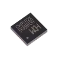
9 Uses0 StarsCH9102X
The CH9102X is a high-speed USB-to-UART bridge IC developed by WCH (Jiangsu Qinheng Microelectronics). It enables seamless communication between a USB host and UART-based embedded systems, making it ideal for programming, debugging, firmware updates, and serial data communication. The device integrates a USB 2.0 Full-Speed interface, an internal clock, power-on reset, and firmware, eliminating the need for an external crystal oscillator. The CH9102X variant supports 3.3 V UART I/O and is widely used on development boards such as ESP32 and other MCU-based designs. Key Features USB 2.0 Full-Speed (12 Mbps) compliant device interface USB-to-UART bridge supporting baud rates from 50 bps to 4 Mbps 3.3 V UART I/O (CH9102X variant) Integrated clock oscillator (no external crystal required) Built-in power-on reset circuit Hardware full-duplex UART with independent TX/RX buffers Supports 5, 6, 7, or 8 data bits Supports None, Odd, Even, Mark, and Space parity Supports RTS/CTS hardware flow control Supports MODEM signals: RTS, CTS, DTR, DSR, DCD, and RI TNOW output for automatic RS-485 transmit/receive control Compatible with built-in CDC drivers and vendor VCP drivers on major operating systems Available in compact RoHS-compliant QFN packages #CH9102X #USBtoUART #USBBridge #UART #SerialConverter #WCH #USB20 #EmbeddedSystems #ESP32 #MCU #RS485 #FirmwareUpdate #Debugging #IoT #PCBDesign
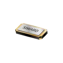
30 Uses0 StarsXTL721-S999-301
32.768 kHz ±20ppm Crystal 9pF 70 kOhms 2-SMD, No Lead The XTL721-S999-301 specification defines the engineering requirements for a crystal oscillator component intended to provide a stable and accurate timing reference for electronic systems. This specification establishes the functional, electrical, mechanical, environmental, and quality requirements necessary to ensure precise frequency generation, reliable operation, and long-term stability in embedded, industrial, communication, and consumer electronic applications. The component is intended for use in applications requiring accurate clock generation and synchronization, including microcontroller-based systems, communication interfaces, digital signal processing, and timing circuits. It provides a highly stable frequency reference with low phase noise and excellent frequency stability to support reliable system operation under varying environmental conditions. Engineering Requirements The crystal component shall be manufactured using high-purity quartz material and precision fabrication processes to ensure consistent resonant frequency characteristics, low aging effects, and dependable long-term performance. The construction shall provide stable oscillation characteristics throughout the specified operating temperature and environmental conditions. Electrical characteristics shall ensure accurate frequency stability, low equivalent series resistance, and reliable oscillation startup when used with compatible oscillator circuits. The component shall maintain stable timing performance under normal supply variations, temperature fluctuations, and continuous operating conditions. Mechanical construction shall be suitable for automated surface-mount assembly and compatible with standard solder reflow manufacturing processes. The package shall provide mechanical robustness and resistance to vibration, mechanical shock, thermal cycling, and handling without degradation of electrical performance or structural integrity. Workmanship shall be free from defects including contamination, package cracking, seal failure, lead deformation, or structural inconsistencies that could adversely affect frequency accuracy or operational reliability. Inspection, validation, and testing shall be performed using calibrated equipment and controlled quality procedures to verify compliance with engineering and manufacturing requirements. Any deviation from this specification shall require formal engineering evaluation, documented technical justification, and approval through the established engineering change control process before implementation. Documentation Supporting documentation shall include engineering drawings, frequency performance specifications, electrical characterization reports, qualification records, inspection reports, reliability data, material declarations, and revision-controlled manufacturing documentation. All documentation shall be maintained under formal configuration management and quality assurance systems to ensure complete product traceability. Revision Control Any modification to this specification shall be managed through the formal engineering change management process. All revisions shall undergo technical review, validation, and approval before release to ensure continued compliance with design intent and applicable engineering standards. #EngineeringSpecification #CrystalOscillator #QuartzCrystal #TimingDevice #ClockGenerator #EmbeddedSystems #IndustrialElectronics #FrequencyControl #QualityAssurance #EngineeringDocumentation
0 Uses0 StarsBSC030N10NS5SCATMA1
N-Channel 100 V 171A (Tc) 188W (Tc) Surface Mount PG-WSON-8-2 The BSC030N10NS5SCATMA1 specification defines the engineering requirements for an N-channel power MOSFET designed for high-efficiency switching and power management applications. This specification establishes the functional, electrical, mechanical, thermal, environmental, and quality requirements necessary to ensure reliable switching performance, low conduction losses, and long-term operational stability in power electronic systems. The device is intended for use in DC-DC converters, synchronous rectification circuits, motor control systems, battery management systems, power distribution modules, and industrial electronic equipment. It provides low on-state resistance, fast switching characteristics, and efficient power handling, making it suitable for high-frequency and high-current applications requiring optimized efficiency and thermal performance. Engineering Requirements The power MOSFET shall be manufactured using advanced semiconductor fabrication processes and qualified materials to ensure consistent electrical characteristics, high switching efficiency, and reliable long-term operation. The device shall maintain stable performance under specified voltage, current, and environmental operating conditions. Electrical characteristics shall provide low on-state resistance, high current-carrying capability, low gate charge, and fast switching performance to minimize conduction and switching losses. The device shall maintain stable operation during repetitive switching cycles, transient load conditions, and dynamic power management applications. Thermal performance shall support efficient heat dissipation through the package structure and printed circuit board interface. The component shall maintain electrical integrity and operational reliability within the specified junction temperature range during continuous and intermittent high-power operation. Mechanical construction shall be suitable for automated surface-mount assembly and compatible with standard solder reflow manufacturing processes. The package shall withstand vibration, thermal cycling, mechanical handling, and environmental exposure without degradation of electrical or mechanical performance. Workmanship shall be free from defects including contamination, cracks, bond failures, package deformation, or structural inconsistencies. Inspection, validation, and testing shall be conducted using calibrated equipment and controlled quality procedures to verify compliance with all applicable engineering and manufacturing requirements. Any deviation from this specification shall require formal engineering evaluation, documented technical justification, and approval through the established engineering change control process. Documentation Supporting documentation shall include engineering drawings, electrical performance specifications, thermal characterization reports, qualification records, inspection reports, material declarations, reliability data, and revision-controlled manufacturing documentation. All documentation shall be maintained under formal configuration management and quality assurance systems to ensure complete product traceability. Revision Control Any modification to this specification shall be managed through the formal engineering change management process. All revisions shall undergo technical review, validation, and approval before implementation to ensure continued compliance with design intent and applicable engineering standards. #EngineeringSpecification #PowerMOSFET #NChannelMOSFET #PowerElectronics #PowerManagement #MotorControl #DCDCConverter #Semiconductor #QualityAssurance #EngineeringDocumentation #commonpartslibrary #transistor #mosfet
0 Uses0 StarsMSPM0C1104S8YCJR
ARM® Cortex®-M0+ MSPM0 C Microcontroller IC 32-Bit 24MHz 16KB (16K x 8) FLASH 8-DSBGA (0.86x1.6) MSPM0C110x microcontrollers (MCUs) are part of the MSP highly-integrated ultra-low-power 32-bit MCU family based on the enhanced Arm® Cortex®-M0+ core platform operating at up to 24MHz frequency. These costoptimized MCUs offer high-performance analog peripheral integration, support extended temperature ranges from -40°C to 125°C, and operate with supply voltages from 1.62V to 3.6V. The MSPM0C110x devices provide up to 16KB embedded flash program memory with 1KB SRAM. These MCUs incorporate a high-speed on-chip oscillator with an accuracy from -2% to +1.2%, eliminating the need for an external crystal. Additional features include a 1-channel DMA, CRC-16 accelerator, and a variety of highperformance analog peripherals such as one 12-bit 1.5Msps ADC with VDD as the voltage reference, and an on-chip temperature sensor. These devices also offer intelligent digital peripherals such as one 16-bit advanced timer, two 16-bit general purpose timer, one windowed watchdog timer, and a variety of communication peripherals including one UART, one SPI, and one I2C. These communication peripherals offer protocol support for LIN, IrDA, DALI, Manchester, smart card, SMBus, and PMBus. The TI MSPM0 family of low-power MCUs consists of devices with varying degrees of analog and digital integration let customers find the MCU that meets their project needs. The architecture combined with extensive low-power modes is optimized to achieve extended battery life in portable measurement applications. MSPM0C110x MCUs are supported by an extensive hardware and software ecosystem with reference designs and code examples to get the design started quickly. Development kits include a LaunchPad™ kit available for purchase and design files for a target-socket board. TI also provides a free MSP Software Development Kit (SDK), which is available as a component of Code Composer Studio™ IDE desktop and cloud version within the TI Resource Explorer. MSPM0 MCUs are also supported by extensive online collateral, training with MSP Academy, and online support through the TI E2E™ support forums. Features • Core – Arm® 32-bit Cortex®-M0+ CPU, frequency up to 24MHz • Operating characteristics – Extended temperature: –40°C to 125°C – Wide supply voltage range: 1.62V to 3.6V • Memories – Up to 16KB of flash – 1KB of SRAM • High-performance analog peripherals – One analog-to-digital converter (ADC) with up to 10 total external channels, 1.7Msps at 10 bit or 1.5Msps at 12 bit with VDD as the voltage reference – Configurable 1.4V or 2.5V internal ADC voltage reference (VREF) – Integrated temperature sensor – Integrated supply monitor • Optimized low-power modes – RUN: 87µA/MHz – STOP: 609µA at 4MHz, 311µA at 32kHz – STANDBY: 5µA with SRAM retention – SHUTDOWN: 200nA • Intelligent digital peripherals – 1-channel DMA controller dedicated for ADC – Three timers supporting up to 14 PWM channels • One 16-bit advanced timers with deadband support up to 8 PWM channels • One 16-bit general purpose timer with 4 capture/compares • One 16-bit general purpose timer with 2 capture/compares – Windowed watchdog timer – BEEPER generating 1kHz, 2kHz, 4kHz, or 8kHz square wave to drive the external beeper • Enhanced communication interfaces – One UART interface supporting LIN, IrDA, DALI, smart card, Manchester and low-power operation in STANDBY mode – One I2C interface supporting FM+ (1Mbps), SMBus, PMBus, and wakeup from STOP mode – One SPI supporting up to 12Mbps • Clock system – Internal 24MHz oscillator with an accuracy from -2% to +1.2% (SYSOSC) – Internal 32kHz low-frequency oscillator (LFOSC) • Data integrity – Cyclic redundancy checker (CRC-16) • Flexible I/O features – Up to 18 GPIOs – Two 5V-tolerant open-drain IOs • Development support – 2-pin serial wire debug (SWD) • Package options – 20-pin TSSOP (PW) – 20-pin VSSOP (DGS) – 20-pin WQFN (RUK) – 16-pin SOT (DYY) – 8-pin SOT (DDF) – 8-pin WSON (DSG) – 8-pin DSBGA (YCJ) • Family members (also see Device Comparison) – MSPS003F4: 16KB of flash, 1KB of RAM – MSPS003F3: 8KB of flash, 1KB of RAM – MSPM0C1104: 16KB of flash, 1KB of RAM – MSPM0C1103: 8KB of flash, 1KB of RAM • Development kits and software (also see Tools and Software) – LP-MSPM0C1104 LaunchPad™ development kit – MSP Software Development Kit (SDK) 2 Applications • Battery charging and management • Power supplies and power delivery • Personal electronics • Building security and fire safety • Connected peripherals and printers • Grid infrastructure • Smart metering • Communication modules • Medical and healthcare • Lighting #MSPM0C1104S8YCJR #MSPM0C1104 #TexasInstruments #CortexM0Plus #Microcontroller #EmbeddedSystems #LowPowerMCU #IoT #WearableDevices #IndustrialControl #ConsumerElectronics #ADC #UART #SPI #I2C #PWM #TI #ElectronicsDesign #PCBDesign #EmbeddedDevelopment
2 Uses0 StarsPCM1822IRTER
ADC, Audio 32 b 8k ~ 192k I2S 20-WQFN (3x3) The PCM1822 is a high-performance, Burr-Brown™ audio analog-to-digital converter (ADC) that supports simultaneous sampling of up to two analog channels. The device supports single-ended and differential line and microphone inputs with a 1-VRMS full-scale signal. The device integrates a phase-locked loop (PLL), a DC removal high-pass filter (HPF), and supports sample rates up to 192 kHz. The device supports time-division multiplexing (TDM) or I2S audio formats, selectable with the hardware pin level. Additionally, the PCM1822 supports master and slave mode selection for the audio bus interface operation. These integrated high-performance features, along with the ability to be powered from a single supply of 3.3 V, make the device an excellent choice for costsensitive, space-constrained audio systems in far-field microphone recording applications. The PCM1822 is specified from –40°C to +125°C, and is offered in a 20-pin WQFN package. Features • Stereo high-performance ADC: – 2-channel analog microphones or line-in • ADC line and microphone differential and singleended input performance: – PCM1822 dynamic range: • 117-dB, dynamic range enhancer enabled • 111-dB, dynamic range enhancer disabled – THD+N: –95 dB • 1-VRMS full-scale input • ADC sample rate (fS) = 8 kHz to 192 kHz • Hardware pin control configurations • Linear-phase or low-latency filter selection • Flexible audio serial data interface: – Master or slave interface selection – 32-bits, 2-channel TDM – 32-bits, 2-channel I2S • Automatic power-down upon loss of audio clocks • Integrated high-performance audio PLL • Single-supply operation: 3.3 V • I/O-supply operation: 3.3 V or 1.8 V • Power consumption for 3.3-V AVDD supply: – 19.6 mW/channel at 16-kHz sample rate – 21.3 mW/channel at 48-kHz sample rate #CommonPartsLibrary #IntegratedCircuit #PCM1822IRTER #TexasInstruments #AudioADC #StereoADC #BurrBrown #I2S #TDM #AudioElectronics #EmbeddedAudio #SmartSpeaker #AVReceiver #HighResolutionAudio #PCBDesign #ElectronicsDesign #SignalProcessing
2 Uses0 StarsAHT30
Fully calibrated temperature and humidity sensor with digital output and I²C interface The AHT30 is a high-precision digital temperature and humidity sensor developed by AOSONG Electronics. It integrates a capacitive humidity sensing element, a temperature sensor, and a dedicated ASIC in a compact DFN package. The device provides fully calibrated digital output through an I²C interface, offering low power consumption, excellent long-term stability, and reliable performance in demanding environmental conditions. It is widely used in smart home devices, HVAC systems, industrial controls, weather monitoring equipment, IoT devices, and consumer electronics. Key Features Fully calibrated digital temperature and humidity sensor I²C digital communication interface Relative humidity measurement range: 0% to 100% RH Temperature measurement range: -40°C to +85°C High accuracy: up to ±2% RH and ±0.3°C (typical) Wide operating voltage: 2.2 V to 5.5 V Low power consumption Fast response time Excellent long-term stability Strong anti-interference capability Compact DFN package suitable for reflow soldering Optimized ASIC with improved MEMS sensing technology Applications Smart home and IoT devices HVAC and air quality monitoring Weather stations Consumer electronics Medical equipment Industrial monitoring and control systems Refrigerators, dehumidifiers, and air conditioners Hashtags #AHT30 #AOSONG #TemperatureSensor #HumiditySensor #EnvironmentalSensor #I2C #MEMS #SmartHome #IoT #HVAC #IndustrialAutomation #WeatherMonitoring #EmbeddedSystems #ElectronicsDesign #PCBDesign
0 Uses0 Stars