Diodes
A diode is a two-terminal electronic component that conducts current primarily in one direction. It is made up of a semiconductor material and has the ability to allow current to pass through it in one direction while blocking current in the opposite direction. Diodes have a wide range of use cases, including rectification, voltage regulation, signal detection, and power management. They are essential components in electronic circuits and can be found in a variety of electronic devices, including computers, smartphones, and appliances. Flux.ai is the world's largest community-driven public library of diodes, with a vast collection of footprints, symbols, datasheets, and simulation models. It is a valuable resource for anyone looking to learn about or work with diodes. Whether you are a student, engineer, or hobbyist, you can find the information and resources you need at Flux.ai to help you understand and work with diodes in your projects.
SS54
DIODE SCHOTTKY 40V SMA(DO-214AC) The SS54 is a surface-mount Schottky barrier rectifier diode commonly used in power management and protection circuits. It is designed for high-speed switching applications and offers low forward voltage drop for improved efficiency in low-voltage systems. The device is widely used in DC-DC converters, reverse polarity protection, freewheeling circuits, and switching power supplies. Key Features Schottky barrier rectifier technology Maximum reverse voltage: 40 V Average forward current: 5 A Low forward voltage drop (typically around 0.55 V) High surge current capability Fast switching speed Surface-mount package (commonly DO-214AB / SMC) Low power loss and high efficiency Suitable for high-frequency applications Guard ring protection for improved reliability RoHS compliant versions available from many manufacturers Typical Applications Switching power supplies DC-DC buck or boost converters Reverse polarity protection Freewheeling / flyback diode applications Battery-powered devices LED drivers Power OR-ing circuits #CommonPartsLibrary #Diode
477 Uses0 StarsULN2803ADW
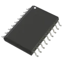
Bipolar (BJT) Transistor Array 8 NPN Darlington 50V 500mA Surface Mount 18-SOIC The ULN2803ADW is a high-voltage, high-current Darlington transistor array designed for interfacing low-level digital logic circuits with high-power loads. The device integrates eight NPN Darlington pairs with common-emitter outputs and suppression diodes for inductive load driving. It is commonly used in relay drivers, LED matrix control, solenoid actuation, motor drivers, lamp control, and industrial automation interfaces. The integrated clamp diodes enable direct driving of inductive loads without requiring additional external protection circuitry. The input stage is compatible with standard TTL and CMOS logic levels, making the device suitable for microcontroller, FPGA, and processor-based systems. The ULN2803ADW provides compact multi-channel switching capability in a wide-body SOIC surface-mount package optimized for automated assembly and high-density PCB layouts. Key Features Eight-channel NPN Darlington transistor array High-current sink driver outputs Integrated flyback suppression diodes TTL and CMOS compatible inputs Open-collector outputs Suitable for inductive and resistive loads High output voltage capability Parallel output operation supported for increased current handling Wide operating voltage range Surface-mount SOIC wide-body package Industrial and embedded control application support Electrical Characteristics Darlington transistor output configuration High DC current gain Low input current requirement Common-cathode clamp diode structure Open-collector output topology Logic-level input compatibility High-voltage output tolerance Multi-channel simultaneous switching support Applications Relay and solenoid drivers Stepper motor interfaces LED and lamp driving Industrial automation systems PLC output stages Embedded control systems Printer and actuator control Automotive electronics Logic buffer and level shifting applications Package Information Package Type: SOIC Wide Body Mounting Type: Surface Mount Multi-pin integrated driver package RoHS compliant options available #commonpartslibrary #integratedcircuit #driveric #darlingtonarray #powermanagement #industrialelectronics #embeddedhardware #relaydriver #motorcontrol #automationelectronics
82 Uses0 StarsTPS259474LRPWR
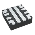
IC SURGE STOPPER 2.7V~23V VQFN-10-HR(2x2) The TPS25947xx family of eFuses is a highly integrated circuit protection and power management solution in a small package. The devices provide multiple protection modes using very few external components and are a robust defense against overloads, short-circuits, voltage surges, reverse polarity and excessive inrush current. With integrated back-to-back FETs, reverse current flow from output to input is blocked at all times, making the devices an excellent choice for power MUX/ORing applications as well as systems which need load side energy hold up storage in case input power supply fails. The devices use linear ORing based scheme to establish an almost zero DC reverse current and emulate ideal diode behavior with minimum forward voltage drop and power dissipation. Output slew rate and inrush current can be adjusted using an external capacitor. Loads are protected from input overvoltage conditions either by clamping the output to a safe fixed maximum voltage (pin selectable), or by cutting off the output if input exceeds an adjustable overvoltage threshold. The devices respond to output overload by actively limiting the current or breaking the circuit. The output current limit threshold as well as the transient overcurrent blanking timer are user adjustable. The current limit control pin also functions as an analog load current monitor. The devices are available in a 2mm × 2mm, 10- pin HotRod™ QFN package for improved thermal performance and reduced system footprint. The devices are characterized for operation over a junction temperature range from –40°C to +125°C. • Wide operating input voltage range: 2.7V to 23V – 28V absolute maximum – Withstands negative voltages up to –15V • Integrated back-to-back FETs with low onresistance: RON = 28.3mΩ (typical) • Ideal diode operation with true reverse-current blocking • Fast overvoltage protection – Overvoltage clamp (OVC) with pin-selectable threshold (3.8V, 5.7V, 13.8V) and 5μs (typical) response time OR – Adjustable overvoltage lockout (OVLO) with 1.2μs (typical) response time • Overcurrent protection with load current monitor output (ILM) – Active current limit OR circuit-breaker options – Adjustable threshold (ILIM) 0.5A to 6A • ±10% accuracy for ILIM > 1A – Adjustable transient blanking timer (ITIMER) to allow peak currents up to 2 × ILIM – Output load current monitor accuracy: ±6% (IOUT ≥ 1A) • Fast-trip response for short-circuit protection – 500ns (typical) response time – Adjustable (2 × ILIM) and fixed thresholds • Active high enable input with adjustable undervoltage lockout threshold (UVLO) • Adjustable output slew rate control (dVdt) • Overtemperature protection • Digital outputs – Priority power MUX control (AUXOFF) and fault indication (FLT) or – Power Good indication (PG) with adjustable threshold (PGTH) • UL 2367 recognition – File No. E339631 – RILM ≥ 750Ω • IEC 62368-1 CB certified • Small footprint: QFN 2mm × 2mm, 0.45mm pitch #CommonPartsLibrary #IntegratedCircuit #PowerManagement
437 Uses0 StarsUSBLC6-2SC6
ESD DIODE 15VC SOT-23-6 The UMW USBLC6-2SC6 is a low-capacitance TVS/ESD protection diode array designed to protect high-speed data interfaces such as USB 2.0 and Ethernet from electrostatic discharge (ESD), electrical fast transients (EFT), and surge events. It integrates dual protection channels in a compact SOT-23-6 package, making it suitable for space-constrained portable and embedded designs. Key Features Dual-line ESD protection for high-speed signal interfaces Supports USB 2.0, 10/100 Ethernet, and other sensitive data lines Very low capacitance (~0.8 pF typical) to preserve signal integrity Operating voltage: 5 V Low clamping voltage for improved downstream IC protection IEC 61000-4-2 ESD protection: ±30 kV air discharge ±30 kV contact discharge IEC 61000-4-4 EFT protection up to 40 A (5/50 ns) IEC 61000-4-5 surge protection up to 6 A (8/20 µs) Peak pulse power capability: 150 W Ultra-low leakage current in the nA range Fast response time (<1 ns typical) Compact SOT-23-6 surface-mount package RoHS, Pb-free, and halogen-free compliant Typical Applications USB data line protection Ethernet interfaces Portable electronics Notebook and desktop PCs Digital cameras Embedded systems and microcontroller USB ports #CommonPartsLibrary #TVS-Diode
3.1k Uses0 StarsLM66100-Q1
Automotive 1.5-V to 5.5-V, 1.5-A, 0.5-µA IQ ideal diode with integrated FET The LM66100-Q1 is a Single-Input, Single-Output (SISO) integrated ideal diode that is well suited for a variety of applications. The device contains a Pchannel MOSFET that can operate over an input voltage range of 1.5 V to 5.5 V and can support a maximum continuous current of 1.5 A. The chip enable works by comparing the CE pin voltage to the input voltage. When the CE pin voltage is higher than VIN, the device disables and the MOSFET is off. When the CE pin voltage is lower, the MOSFET is on. The LM66100-Q1 also comes with reverse polarity protection (RPP) that can protect the device from a miswired input, such as a reversed battery. Two LM66100-Q1 devices can be used in an ORing configuration similar to a dual diode ORing implementation. In this configuration, the devices pass the highest input voltage to the output while blocking reverse current flow into the input supplies. These devices can compare input and output voltages to make sure that reverse current is blocked through an internal voltage comparator. The LM66100-Q1 is available in a standard SC-70 package characterized for operation over a junction temperature range of –40°C to 150°C. 1 Features • AEC-Q100 qualified for automotive applications: – Device temperature grade 1: –40°C to 125°C ambient operating temperature range • Wide operating voltage range: 1.5 V–5.5 V • Reverse voltage standoff on VIN: –6-V absolute maximum • Maximum continuous current (IMAX): 1.5 A • On-Resistance (RON): – 5-V VIN = 79 mΩ (typical) – 3.6-V VIN = 91 mΩ (typical) – 1.8-V VIN = 141 mΩ (typical) • Comparator chip enable (CE) • Channel status indication (ST) • Low current consumption: – 3.6-V VIN shutdown current (ISD,VIN): 120 nA (typical) – 3.6-V VIN quiescent current (IQ, VIN): 150 nA (typical)
96 Uses0 StarsTPD2E2U06DCKR
12.4V (Typ) Clamp 5.5A (8/20µs) Ipp Tvs Diode Surface Mount SC-70-3 TPD2E2U06 USB ESD The TPD2E2U06 is a dual-channel low capacitance TVS diode ESD protection device. The device offers ±25-kV contact and ±30-kV air-gap ESD protection in accordance with the IEC 61000-4-2 standard. The 1.5-pF line capacitance of the TPD2E2U06 makes the device suitable for a wide range of applications. Typical application interfaces are USB 2.0, LVDS, and I 2C™. Features 1• IEC 61000-4-2 Level 4 – ±25 kV (Contact discharge) – ±30 kV (Air-gap discharge) • IEC 61000-4-5 Surge protection – 5.5-A Peak pulse current (8/20 µs Pulse) • IO Capacitance 1.5 pF (Typ) • DC Breakdown voltage 6.5 V (Min) • Ultra-Low leakage current 10 nA (Max) • Low ESD clamping voltage • Industrial temperature range: –40°C to +125°C • Small easy-to-route DRL and DCK package #CommonPartsLibrary #TVS-diode
399 Uses0 StarsLM74700QDDFRQ1
OR Controller N+1 ORing Controller N-Channel 1:1 TSOT-23-8 The LM74700QDDFRQ1 is an automotive-qualified ideal diode controller designed to provide reverse polarity protection, reverse current blocking, and input power path management in low-voltage DC power systems. The device controls an external N-channel MOSFET to emulate an ideal diode with very low forward voltage drop and reduced power dissipation compared to conventional Schottky diodes. It is optimized for automotive and industrial applications requiring robust protection against negative supply voltages, load dump conditions, and reverse battery events. The controller supports wide input voltage operation and integrates fast response circuitry for fault handling and transient protection. The device is suitable for power OR-ing, hot-swap, redundant power supply systems, and battery-connected applications where efficiency, reliability, and thermal performance are critical. Engineering Specification Device Type Automotive ideal diode controller with reverse battery and reverse current protection Qualification Standard AEC-Q100 qualified for automotive applications Control Topology External N-channel MOSFET controller for ideal diode operation Input Voltage Range Supports wide automotive and industrial supply voltage ranges Reverse Polarity Protection Provides protection against negative input voltage conditions and reverse battery connection Reverse Current Blocking Actively prevents reverse current flow during output-to-input fault conditions Forward Voltage Drop Low conduction losses through external MOSFET control for high-efficiency power delivery Transient Protection Capable of handling automotive transient events including load dump conditions Gate Drive Control Integrated gate driver optimized for fast MOSFET switching and protection response Power Path Management Supports power OR-ing and redundant supply architectures Fault Response Fast turn-off during reverse current and fault events Current Consumption Low operating quiescent current suitable for always-on systems Thermal Performance Designed for efficient thermal operation with external MOSFET-based power dissipation Operating Temperature Range Automotive-grade extended temperature operation Package Type Small-outline automotive package suitable for compact PCB layouts #commonpartsLibrary #integratedcircuit #powermanagement #orcontroller
848 Uses0 Stars