Oscillators
An oscillator is an electronic circuit that generates a periodic, oscillating signal, often a sine wave or a square wave. Oscillators are used in a wide range of applications, including clocks, radios, and sound synthesis. Flux.ai has the world's largest community-driven public library of oscillators, with footprints, symbols, datasheets, and simulation models. This comprehensive resource allows engineers and designers to easily find the oscillator they need for their specific application and use it with confidence. Whether you are working on a simple clock circuit or a complex radio transmitter, Flux.ai's oscillator library has you covered. So, if you are in need of an oscillator for your next project, be sure to check out Flux.ai's extensive collection.
PCA9685PW,118
LED Driver IC 16 Output Linear PWM Dimming 25mA 28-TSSOP The PCA9685 is an I2C-bus controlled 16-channel LED controller optimized for Red/Green/Blue/Amber (RGBA) color backlighting applications. Each LED output has its own 12-bit resolution (4096 steps) fixed frequency individual PWM controller that operates at a programmable frequency from a typical of 24 Hz to 1526 Hz with a duty cycle that is adjustable from 0 % to 100 % to allow the LED to be set to a specific brightness value. All outputs are set to the same PWM frequency. Each LED output can be off or on (no PWM control), or set at its individual PWM controller value. The LED output driver is programmed to be either open-drain with a 25 mA current sink capability at 5 V or totem pole with a 25 mA sink, 10 mA source capability at 5 V. The PCA9685 operates with a supply voltage range of 2.3 V to 5.5 V and the inputs and outputs are 5.5 V tolerant. LEDs can be directly connected to the LED output (up to 25 mA, 5.5 V) or controlled with external drivers and a minimum amount of discrete components for larger current or higher voltage LEDs. The PCA9685 is in the new Fast-mode Plus (Fm+) family. Fm+ devices offer higher frequency (up to 1 MHz) and more densely populated bus operation (up to 4000 pF). Although the PCA9635 and PCA9685 have many similar features, the PCA9685 has some unique features that make it more suitable for applications such as LCD or LED backlighting and Ambilight: • The PCA9685 allows staggered LED output on and off times to minimize current surges. The on and off time delay is independently programmable for each of the 16 channels. This feature is not available in PCA9635. • The PCA9685 has 4096 steps (12-bit PWM) of individual LED brightness control. The PCA9635 has only 256 steps (8-bit PWM). • When multiple LED controllers are incorporated in a system, the PWM pulse widths between multiple devices may differ if PCA9635s are used. The PCA9685 has a programmable prescaler to adjust the PWM pulse widths of multiple devices. • The PCA9685 has an external clock input pin that will accept user-supplied clock (50 MHz max.) in place of the internal 25 MHz oscillator. This feature allows synchronization of multiple devices. The PCA9635 does not have external clock input feature. • Like the PCA9635, PCA9685 also has a built-in oscillator for the PWM control. However, the frequency used for PWM control in the PCA9685 is adjustable from about 24 Hz to 1526 Hz as compared to the typical 97.6 kHz frequency of the PCA9635. This allows the use of PCA9685 with external power supply controllers. All bits are set at the same frequency. • The Power-On Reset (POR) default state of LEDn output pins is LOW in the case of PCA9685. It is HIGH for PCA9635. #CommonPartsLibrary #IntegratedCircuit #PowerManagement
216 Uses0 StarsSN74HC14APWR
Inverter IC 6 Channel Schmitt Trigger 14-TSSOP The SN74HC14APWR is a high-speed CMOS hex Schmitt-trigger inverter manufactured by Texas Instruments. This device integrates six independent inverting Schmitt-trigger gates designed to provide clean digital signal transitions from slow-rising or noisy input signals. It is commonly used for waveform shaping, signal conditioning, switch debouncing, pulse generation, and oscillator circuits in embedded systems and digital electronics. The device operates over a wide supply voltage range and offers low power consumption with high noise immunity characteristics. The Schmitt-trigger input architecture provides hysteresis, improving signal stability in noisy environments and ensuring reliable logic switching performance. The SN74HC14APWR is widely used in microcontroller interfaces, communication systems, industrial electronics, consumer devices, and general-purpose digital logic applications. Engineering Specification Device Type Hex Schmitt-Trigger Inverter Logic Function Inverting Schmitt-trigger gate Number of Channels Six independent inverter gates Logic Family High-Speed CMOS (HC) Supply Voltage Range Compatible with standard CMOS voltage levels Input Characteristics Schmitt-trigger inputs with hysteresis for noise immunity Output Characteristics CMOS push-pull outputs capable of driving standard digital loads Propagation Delay High-speed switching performance suitable for digital timing applications Power Consumption Low static and dynamic power consumption Noise Immunity High noise margin due to Schmitt-trigger input structure Operating Temperature Range Industrial operating temperature capability Package Type TSSOP surface-mount package Mounting Type Surface mount technology Applications Signal conditioning Switch debouncing Clock shaping Oscillator circuits Pulse generation Microcontroller interfacing Digital waveform cleanup Industrial control systems Manufacturer Texas Instruments #commonpartslibrary #integratedcircuit #logicic #schmitttrigger #hexinverter #digitalelectronics #embeddedhardware #signalconditioning #texasinstruments #cmoslogic #surfaceountcomponents #electronicsdesign
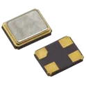
51 Uses0 StarsNX1612SA-32MHZ-STD-CIS-3
Small and thin surface-mount crystal units NX1612SA-32MHZ-STD-CIS-3 is a compact surface-mount quartz crystal oscillator designed for stable clock generation in embedded electronic systems and wireless communication devices. Manufactured in a miniature ceramic package, this crystal provides precise frequency control with low phase noise and high frequency stability, making it suitable for microcontrollers, RF modules, IoT devices, and portable electronics. The device operates at a nominal frequency of thirty-two megahertz and is optimized for low power consumption and reliable startup characteristics. Its compact footprint enables integration into high-density PCB layouts while maintaining strong resistance to environmental stress and mechanical vibration. The crystal is compatible with standard oscillator circuits and supports stable operation across industrial temperature ranges. This component is commonly used in timing reference applications, communication systems, sensor modules, wearable devices, and battery-powered embedded platforms requiring accurate and stable clock signals. #commonpartslibrary #crystaloscillator #timingdevice #frequencycontrol #embeddedhardware #wirelesssystems #rfdesign #iotdevices #electronicscomponents #surfacemountdevice
40 Uses0 StarsADS1256IDBT
USB-A (USB TYPE-A) USB 2.0 Receptacle Connector 4 Position Through Hole, Right Angle The ADS1256IDBT is a high-precision, low-noise, 24-bit analog-to-digital converter manufactured by Texas Instruments. It is designed for high-resolution measurement applications requiring exceptional accuracy, low drift, and programmable data rates. The device integrates a low-noise programmable gain amplifier, a precision delta-sigma ADC core, and a flexible multiplexer that supports multiple differential or single-ended analog inputs. The converter is optimized for industrial process control, sensor measurement, weigh scales, data acquisition systems, temperature monitoring, and portable instrumentation. Its integrated digital filtering and selectable gain settings enable direct interfacing with low-level sensors such as strain gauges, thermocouples, RTDs, and bridge sensors without requiring extensive external signal conditioning. The ADS1256IDBT supports SPI-compatible serial communication and operates with low power consumption while maintaining excellent dynamic performance and high effective resolution. The device provides programmable output data rates suitable for both low-speed precision measurements and higher-speed acquisition systems. Device Features 24-bit delta-sigma analog-to-digital converter Low-noise programmable gain amplifier Eight single-ended or four differential analog input channels Programmable gain settings from 1 to 64 Programmable data output rates SPI-compatible serial interface Integrated digital filter for noise reduction Low offset drift and gain drift Internal oscillator support Sensor burnout detection capability Self-calibration and system calibration functions Low power operation Wide analog supply voltage range Excellent 50 Hz and 60 Hz rejection performance Electrical Characteristics Resolution of 24 bits Maximum data rate up to 30 kSPS Differential input architecture Input multiplexer for multi-channel acquisition Low RMS noise performance High common-mode rejection ratio High power-supply rejection ratio Programmable gain amplifier integrated on-chip Internal reference support with external reference capability Interface and Control SPI-compatible digital communication interface Configurable control registers Read and write register functionality Synchronization and standby control support Hardware reset capability Interrupt and data-ready signaling support Package Information Manufacturer package designation: DBT Package type: TSSOP Surface-mount device Fine-pitch lead configuration Industrial temperature grade device Applications Precision data acquisition systems Industrial automation and control Weigh scales and bridge sensors Temperature measurement systems Pressure sensing applications Portable instrumentation Medical instrumentation Laboratory measurement equipment Energy monitoring systems Process monitoring and control Manufacturer Information Manufacturer: Texas Instruments Manufacturer Part Number: ADS1256IDBT Product Category: Precision Analog-to-Digital Converter RoHS compliant device #commonpartslibrary #integratedcircuit #analog #adc #deltasigma #precisionadc #sensorinterface #dataacquisition #industrialautomation #instrumentation #signalconditioning #texasinstruments #spiinterface #mixedsignal #measurementsystems
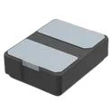
65 Uses0 StarsNX3225GD-8MHZ-STD-CRA-3
CRYSTAL 8MHz 8pF SMD The NX3225GD-8MHZ-STD-CRA-3 is an automotive-grade surface-mount quartz crystal unit from NDK designed to provide a stable 8 MHz clock reference for microcontrollers, automotive ECUs, and embedded systems. It belongs to the NX3225GD series and is optimized for high reliability under harsh environmental conditions. Key Features 8 MHz fundamental-mode crystal Compact 3.2 mm × 2.5 mm × 1.0 mm SMD package 8 pF load capacitance ±50 ppm frequency tolerance ±150 ppm frequency stability over temperature Automotive-qualified with AEC-Q200 compliance Wide operating temperature range: −40°C to +150°C Excellent resistance to heat, vibration, shock, and solder cracking Stable startup characteristics in severe environments RoHS compliant Typical Applications Automotive engine control units (ECUs) MCU and CPU clock generation Industrial embedded systems Communication equipment Consumer electronics and IoT devices #CommonPartsLibrary #crystal oscillator #resonator
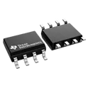
293 Uses0 StarsTLC555IDR
555 Type, Timer/Oscillator (Single) IC 2.1MHz 8-SOIC The TLC555IDR is a low-power CMOS timer device designed as a functional replacement for the standard bipolar 555 timer while providing significantly reduced supply current and improved operating efficiency. The device supports both astable and monostable operating modes and is commonly used for timing generation, pulse shaping, oscillation, PWM generation, delay circuits, and frequency generation applications. The CMOS architecture enables low power consumption, rail-to-rail output capability, and stable timing performance over a wide operating voltage range. The device is suitable for battery-powered systems, portable electronics, industrial controls, instrumentation, consumer products, and embedded electronic designs. The TLC555IDR is supplied in a compact SOIC surface-mount package intended for automated PCB assembly and space-constrained applications. Electrical Characteristics CMOS low-power timer architecture Functional equivalent to standard 555 timer devices Wide operating supply voltage range Low quiescent supply current High input impedance Rail-to-rail output swing capability Stable threshold and trigger levels Compatible with TTL and CMOS logic levels Capable of astable and monostable operation Adjustable duty cycle and frequency operation High output drive capability for direct interfacing Low noise and improved switching performance compared to bipolar 555 timers Functional Features Precision timing generation Oscillator and clock generation Pulse-width modulation support One-shot pulse generation Delay timer implementation Missing pulse detection Frequency divider implementation Sequential timing control LED flashing and tone generation PWM motor and power control applications Package Information Surface-mount SOIC package Standard tape-and-reel packaging format Compact footprint for automated assembly RoHS compliant device construction Environmental and Operating Conditions Industrial operating temperature range ESD protection handling required Suitable for commercial and industrial embedded systems Designed for low-power electronic applications Typical Applications Timer circuits Pulse generators Oscillators PWM controllers LED flashers Alarm and tone generators Frequency generators Power management timing Embedded control systems Portable battery-powered electronics #commonpartslibrary #integratedcircuit #timer #oscillator
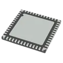
80 Uses0 StarsdsPIC33CK256MP205-I/M4
dsPIC dsPIC™ 33CK, Functional Safety (FuSa) Microcontroller IC 16-Bit 100MHz 256KB (256K x 8) FLASH 48-UQFN (6x6) 28/36/48/64/80-Pin Digital Signal Controllers with High-Resolution PWM and CAN Flexible Data (CAN FD) Operating Conditions • 3.0V to 3.6V, -40°C to +125°C, DC to 100 MIPS • 3.0V to 3.6V, -40°C to +150°C, DC to 70 MIPS Core: 16-Bit dsPIC33CK CPU • 32-256 Kbytes of Program Flash with ECC and 8-24K RAM • Fast 6-Cycle Divide • LiveUpdate • Code Efficient (C and Assembly) Architecture • 40-Bit Wide Accumulators • Single-Cycle (MAC/MPY) with Dual Data Fetch • Single-Cycle, Mixed-Sign MUL Plus Hardware Divide • 32-Bit Multiply Support • Four Sets of Interrupt Context Saving Registers which Include Accumulator and STATUS for Fast Interrupt Handling • Zero Overhead Looping • RAM Memory Built-In Self-Test (MBIST) Clock Management • Internal Oscillator • Programmable PLLs and Oscillator Clock Sources • Reference Clock Output • Fail-Safe Clock Monitor (FSCM) • Fast Wake-up and Start-up • Backup Internal Oscillator Power Management • Low-Power Management Modes (Sleep, Idle, Doze) • Integrated Power-on Reset and Brown-out Reset High-Speed PWM • Eight PWM Pairs • Up to 250 ps PWM Resolution • Dead Time for Rising and Falling Edges • Dead-Time Compensation • Clock Chopping for High-Frequency Operation • PWM Support for: - DC/DC, AC/DC, inverters, PFC, lighting - BLDC, PMSM, ACIM, SRM motors • Fault and Current Limit Inputs • Flexible Trigger Configuration for ADC Triggering Timers/Output Compare/Input Capture • One General Purpose Timer • Peripheral Trigger Generator (PTG): - Up to 15 trigger sources to other peripheral modules - CPU independent state machine-based instruction sequencer • Nine MCCP/SCCP modules which Include Timer, Capture/Compare and PWM: - One MCCP - Eight SCCPs - 16 or 32-bit time base - 16 or 32-bit capture - 4-deep capture buffer • Fully Asynchronous Operation, Available in Sleep Modes #CommonPartsLibrary #IntegratedCircuit #Microcontroller #DSPIC33CK256MP
10 Uses0 StarsSTM32F407VGT6
ARM Microcontrollers - MCU ARM M4 1024 FLASH 168 Mhz 192kB SRAM 100-LQFP (14x14) Arm® Cortex®-M4 32b MCU+FPU, 210DMIPS, up to 1MB Flash/192+4KB RAM, USB OTG HS/FS, Ethernet, 17 TIMs, 3 ADCs, 15 comm. interfaces & camera • Core: Arm® 32-bit Cortex®-M4 CPU with FPU, Adaptive real-time accelerator (ART Accelerator) allowing 0-wait state execution from Flash memory, frequency up to 168 MHz, memory protection unit, 210 DMIPS/ 1.25 DMIPS/MHz (Dhrystone 2.1), and DSP instructions • Memories – Up to 1 Mbyte of Flash memory – Up to 192+4 Kbytes of SRAM including 64- Kbyte of CCM (core coupled memory) data RAM – 512 bytes of OTP memory – Flexible static memory controller supporting Compact Flash, SRAM, PSRAM, NOR and NAND memories • LCD parallel interface, 8080/6800 modes • Clock, reset and supply management – 1.8 V to 3.6 V application supply and I/Os – POR, PDR, PVD and BOR – 4-to-26 MHz crystal oscillator – Internal 16 MHz factory-trimmed RC (1% accuracy) – 32 kHz oscillator for RTC with calibration – Internal 32 kHz RC with calibration • Low-power operation – Sleep, Stop and Standby modes –VBAT supply for RTC, 20×32 bit backup registers + optional 4 KB backup SRAM • 3×12-bit, 2.4 MSPS A/D converters: up to 24 channels and 7.2 MSPS in triple interleaved mode • 2×12-bit D/A converters • General-purpose DMA: 16-stream DMA controller with FIFOs and burst support • Up to 17 timers: up to twelve 16-bit and two 32- bit timers up to 168 MHz, each with up to 4 IC/OC/PWM or pulse counter and quadrature (incremental) encoder input • Debug mode – Serial wire debug (SWD) & JTAG interfaces – Cortex-M4 Embedded Trace Macrocell™ • Up to 140 I/O ports with interrupt capability – Up to 136 fast I/Os up to 84 MHz – Up to 138 5 V-tolerant I/Os • Up to 15 communication interfaces – Up to 3 × I2C interfaces (SMBus/PMBus) – Up to 4 USARTs/2 UARTs (10.5 Mbit/s, ISO 7816 interface, LIN, IrDA, modem control) – Up to 3 SPIs (42 Mbits/s), 2 with muxed full-duplex I2S to achieve audio class accuracy via internal audio PLL or external clock – 2 × CAN interfaces (2.0B Active) – SDIO interface • Advanced connectivity – USB 2.0 full-speed device/host/OTG controller with on-chip PHY – USB 2.0 high-speed/full-speed device/host/OTG controller with dedicated DMA, on-chip full-speed PHY and ULPI – 10/100 Ethernet MAC with dedicated DMA: supports IEEE 1588v2 hardware, MII/RMII #CommonPartsLibrary #IntegratedCircuit #Microcontroller #STM32F407
50 Uses0 StarsSTM32F103C8T6
ARM® Cortex® M3 STM32F1 Microcontroller IC 32-Bit Single-Core 72MHz 64KB (64K x 8) FLASH Medium-density performance line Arm®-based 32-bit MCU with 64 or 128 KB Flash, USB, CAN, 7 timers, 2 ADCs, 9 com. interfaces Arm® 32-bit Cortex®-M3 CPU core – 72 MHz maximum frequency, 1.25 DMIPS/MHz (Dhrystone 2.1) performance at 0 wait state memory access – Single-cycle multiplication and hardware division • Memories – 64 or 128 Kbytes of Flash memory – 20 Kbytes of SRAM • Clock, reset and supply management – 2.0 to 3.6 V application supply and I/Os – POR, PDR, and programmable voltage detector (PVD) – 4 to 16 MHz crystal oscillator – Internal 8 MHz factory-trimmed RC – Internal 40 kHz RC – PLL for CPU clock – 32 kHz oscillator for RTC with calibration • Low-power – Sleep, Stop and Standby modes – VBAT supply for RTC and backup registers • 2x 12-bit, 1 µs A/D converters (up to 16 channels) – Conversion range: 0 to 3.6 V – Dual-sample and hold capability – Temperature sensor • DMA – 7-channel DMA controller – Peripherals supported: timers, ADC, SPIs, I 2Cs and USARTs • Up to 80 fast I/O ports – 26/37/51/80 I/Os, all mappable on 16 external interrupt vectors and almost all 5 V-tolerant Debug mode: – Serial wire debug (SWD) and JTAG interfaces • Seven timers – Three 16-bit timers, each with up to 4 IC/OC/PWM or pulse counter and quadrature (incremental) encoder input – 16-bit, motor control PWM timer with dead-time generation and emergency stop – Two watchdog timers (independent and window) – SysTick timer 24-bit downcounter • Up to nine communication interfaces – Up to two I2C interfaces (SMBus/PMBus®) – Up to three USARTs (ISO 7816 interface, LIN, IrDA capability, modem control) – Up to two SPIs (18 Mbit/s) – CAN interface (2.0B Active) – USB 2.0 full-speed interface • CRC calculation unit, 96-bit unique ID • Packages are ECOPACK #commonpartslibrary #integratedcircuit #microcontroller #stm32f1
32 Uses0 Stars