Oscillators
An oscillator is an electronic circuit that generates a periodic, oscillating signal, often a sine wave or a square wave. Oscillators are used in a wide range of applications, including clocks, radios, and sound synthesis. Flux.ai has the world's largest community-driven public library of oscillators, with footprints, symbols, datasheets, and simulation models. This comprehensive resource allows engineers and designers to easily find the oscillator they need for their specific application and use it with confidence. Whether you are working on a simple clock circuit or a complex radio transmitter, Flux.ai's oscillator library has you covered. So, if you are in need of an oscillator for your next project, be sure to check out Flux.ai's extensive collection.
SG3525AN
Buck, Push-Pull Regulator Positive Output Step-Down, Step-Up/Step-Down DC-DC Controller IC 16-DIP SG3525 is a pulse width modulation (PWM) controller IC designed for switch-mode power supply and power conversion control applications. It operates from an 8 V to 35 V supply and integrates a 5.1 V ±1% reference, oscillator with adjustable frequency, error amplifier, PWM comparator, soft-start, undervoltage lockout, and dual totem-pole output stages capable of source/sink drive for external power devices. #STMicroelectronics #SG3525AN #PWMController #SMPS #PowerSupply #PowerManagement #Oscillator #SoftStart #UndervoltageLockout #DualOutput #commonpartslibrary #integratedcircuit #powermanagement #dcdccontroller
72 Uses0 StarsXL1509-5.0E1
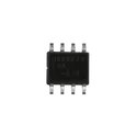
2A 150KHz 40V Buck DC to DC Converter The XL1509-5.0E1 is a fixed frequency PWM buck step-down DC-DC converter capable of driving a load with high efficiency, low ripple, and excellent line and load regulation. It is manufactured by XLSEMI and belongs to the XL1509 product family, a series of fixed-output and adjustable-output step-down switching regulator ICs designed to simplify the design of compact, efficient DC power conversion stages in a wide range of embedded, industrial, and consumer electronics applications. The "5.0" designation in the part number specifies that this variant produces a fixed regulated output voltage of five volts, making it directly suited to powering five-volt logic, microcontrollers, sensors, communication modules, and other standard digital subsystems from higher-voltage DC rails without requiring a linear regulator and its inherent power dissipation penalty. Unikeyic Electronics The XL1509 requires a minimum number of external components, making it simple to use, and includes internal frequency compensation and a fixed-frequency oscillator. The PWM control circuit is able to adjust the duty ratio linearly from zero to one hundred percent. This internal compensation architecture removes the burden of control loop design from the system engineer, which is a common point of complexity in discrete buck converter designs, and allows the device to be implemented with a straightforward application circuit consisting of an input capacitor, an output inductor, a freewheeling Schottky diode, and an output capacitor, without requiring additional feedback network components in the fixed-output version. Unikeyic Electronics The device operates across a wide input voltage range, accepting input rails ranging from just above the output voltage all the way up to the high end of the input range, making it compatible with a variety of common source voltages including twelve-volt, twenty-four-volt, and other industrial bus rails frequently encountered in embedded and industrial power system designs. This wide input range also makes it suitable for battery-powered applications where the supply voltage varies considerably across the battery discharge cycle, as the converter maintains a regulated output throughout the input voltage window. The fixed switching frequency is set internally at a value that represents a practical tradeoff between external component size and switching loss, allowing the use of standard commodity inductors and electrolytic or ceramic output capacitors without requiring unusually large or small values. An enable function and an overcurrent protection function are built inside. When a secondary current limit condition occurs, the operating frequency is reduced to a lower switching frequency, which limits the energy delivered per cycle and prevents damage to the power switch and external components during sustained overload events. This dual-level current protection approach provides both instantaneous peak current limiting and sustained overload protection, improving the robustness of designs built around the device in applications where load transients or fault conditions may cause temporary overcurrent conditions. Unikeyic Electronics The device is housed in a standard eight-pin small-outline integrated circuit surface-mount package, making it compatible with automated pick-and-place and reflow soldering assembly processes and suitable for compact power supply layouts on densely populated PCBs. Spec Sheet Identification Part Number: XL1509-5.0E1 Device Family: XL1509 Buck DC-DC Converter Series Manufacturer: XLSEMI Part Number Decode XL1509: Base device family 5.0: Fixed output voltage — five volts E1: Tape-and-reel packaging variant Functional Classification Device Type: Fixed-frequency PWM step-down buck DC-DC converter IC Topology: Non-synchronous buck converter with internal power switch Output Configuration: Single output, fixed voltage Regulation Method: Fixed-frequency PWM with internal compensation Electrical Characteristics Input Voltage Range: Wide input range, compatible with common industrial and consumer DC bus voltages Output Voltage: Fixed regulated output at five volts Output Current: Continuous rated current class suitable for moderate embedded system loads Switching Frequency: Fixed internal oscillator, mid-frequency class Duty Cycle Range: Adjustable from zero to maximum, internally controlled Minimum Dropout Voltage: Low dropout class Output Ripple: Low ripple characteristic with appropriate external filter components Control & Protection Features Enable Function: Built-in enable control input for power sequencing and shutdown Overcurrent Protection: Integrated primary current limit with frequency fold-back secondary protection Internal Compensation: Built-in frequency compensation, no external compensation network required Feedback: Internal reference for fixed output voltage regulation External Components Required Input Capacitor: Required for input decoupling Output Inductor: Required, standard commodity value Freewheeling Diode: External Schottky diode required Output Capacitor: Required for output filtering Environmental & Qualification Operating Temperature Range: Industrial range, below zero to elevated ambient RoHS Compliance: Yes, Halogen-Free Package Package Type: SOIC-8 (SOP-8) Mounting Method: Surface mount technology (SMT) Packaging Format Supply Format: Tape-and-reel Reel Quantity: Standard production reel quantity Available Variants in XL1509 Family XL1509-3.3E1: Fixed output at regulated lower voltage XL1509-5.0E1: Fixed output at five volts (this device) XL1509-12E1: Fixed output at twelve volts XL1509-ADJE1: Adjustable output version #XL1509 #XL15095 #XLSEMI #BuckConverter #StepDownConverter #DCDCConverter #PWMConverter #SwitchingRegulator #PowerManagement #EmbeddedPower #FixedOutputConverter #FiveVoltRegulator #IndustrialPower #SOIC8 #SurfaceMount #LowRipple #HighEfficiency #SemiconductorIC #EngineeringSpec #ComponentLibrary #CommonPartsLibrary #RoHSCompliant #PCBDesign
15 Uses0 StarsLORA-CC68-915MHz-TCXO
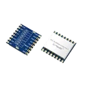
LORA-CC68-915MHz-TCXO is a compact, high-performance LoRa wireless transceiver module from NiceRF based on the Semtech LLCC68 chipset. Operating in the 915 MHz ISM band, it features a high-precision TCXO (Temperature-Compensated Crystal Oscillator) for improved frequency stability, making it ideal for long-range, low-power IoT and industrial wireless communication applications. The module supports LoRa, FSK, and GFSK modulation schemes, provides up to +22 dBm (160 mW) transmit power, and achieves receiver sensitivity as low as -129 dBm for extended communication range. It communicates through an SPI interface and is optimized for battery-powered and low-power systems. Key Features Based on Semtech LLCC68 LoRa transceiver chip 915 MHz ISM band operation High-precision TCXO for enhanced frequency stability Supports LoRa, FSK, and GFSK modulation Up to +22 dBm (160 mW) RF output power Receiver sensitivity up to -129 dBm SPI communication interface Operating voltage: 1.8 V to 3.7 V Low receive current (~6.5 mA typical) Integrated antenna switching circuitry Compact 16 mm × 16 mm SMD package Suitable for long-range and low-power wireless applications FCC-certified 915 MHz version RoHS compliant Typical Applications Smart Metering Industrial Automation Agricultural Monitoring Smart Cities Environmental Sensors Asset Tracking Warehouse Management Remote Control Systems Street Lighting Control Battery-Powered IoT Devices #CommonPartsLibrary #Module #LoRa #LLCC68 #915MHz #TCXO #WirelessModule #RFModule #IoT #IndustrialAutomation #SmartMetering #LongRangeCommunication #LowPowerDesign #SPI #EmbeddedSystems #NiceRF
0 Uses0 StarsPT2272M4
PT2272-M4 is a CMOS remote control decoder IC designed to work with the PT2262 encoder for wireless RF and infrared remote control applications. It decodes incoming encoded signals and provides four momentary data outputs, making it ideal for remote switching, security systems, garage door openers, home automation, and industrial control systems. The "M4" variant features 4 momentary output channels, where outputs remain active only while the corresponding transmitter button is pressed. Key Features CMOS technology for low power consumption 4 momentary data output channels (M4 version) Up to 12 tri-state address pins for secure coding Supports up to 531,441 unique address combinations High noise immunity for reliable operation Wide operating voltage range: 4V to 15V Single-resistor oscillator design Compatible with PT2262 encoder IC Available in DIP and SOP package options Suitable for RF and infrared remote control systems Applications Wireless remote controls Garage door openers Car security systems Home automation equipment Remote-controlled fans and appliances Industrial wireless control systems Remote-controlled toys #CommonPartsLibrary #IntegratedCircuit #PT2272M4 #RemoteControlDecoder #RFDecoder #WirelessControl #HomeAutomation #SecuritySystem #GarageDoorOpener #CMOSIC #PT2262 #IndustrialControl #EmbeddedSystems #ElectronicsDesign
0 Uses0 StarsLAN8770M-I/PRA
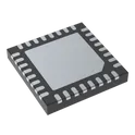
4/4 Transceiver Full MII, RMII 32-VQFN (5x5) ## Engineering Specification ## General Description The **LAN8770M-I/PRA** is a Microchip Technology single-port **100BASE-T1 Ethernet physical layer transceiver** designed for automotive, industrial, and embedded networking applications. It provides Ethernet communication over a single balanced twisted pair and is suitable for compact systems requiring reliable network connectivity, low-power operation, and standard MAC interface support. The device is commonly used in automotive electronic control units, infotainment systems, telematics modules, sensor nodes, industrial control systems, and embedded Ethernet hardware. ## Device Identification Manufacturer Part Number: **LAN8770M-I/PRA** Manufacturer: **Microchip Technology** Product Family: **LAN8770** Device Category: **Integrated Circuit** Device Type: **Ethernet PHY Transceiver** Ethernet Standard: **100BASE-T1** Interface Type: **MII and RMII** Mounting Type: **Surface Mount** Package Type: **VQFN** ## Functional Description The device functions as an Ethernet physical layer transceiver that connects a host controller or microcontroller MAC interface to a single-pair Ethernet physical medium. It handles the analog and digital PHY functions required for 100BASE-T1 communication, allowing embedded systems to transmit and receive Ethernet data over a single twisted pair cable. ## Network and Interface Description The **LAN8770M-I/PRA** supports 100 Mb/s single-pair Ethernet communication and provides MII and RMII host interface options. This allows integration with microcontrollers, processors, gateways, and network controllers that support standard Ethernet MAC interfaces. The device is intended for applications where compact Ethernet connectivity and reduced cabling complexity are required. ## Electrical Description The device is designed for low-voltage operation and supports multiple supply domains according to the manufacturer’s recommended operating conditions. Proper power sequencing, decoupling, reset handling, clocking, and reference layout should be implemented to maintain stable PHY operation and signal integrity. ## Package and Mechanical Description The component is supplied in a compact surface-mount **VQFN package**, suitable for dense printed circuit board assemblies. The package supports automated assembly and is appropriate for space-constrained automotive and industrial electronic designs. ## Control and Diagnostic Description The PHY supports management and configuration through standard control interfaces used in Ethernet designs. It provides status monitoring and configuration capability for link management, operating mode selection, and system-level diagnostics. These features allow the host controller to configure and monitor Ethernet link behavior during operation. ## Automotive and Industrial Suitability The **LAN8770M-I/PRA** is suitable for embedded systems requiring robust single-pair Ethernet communication. It is applicable to automotive networking, telematics, infotainment, advanced driver assistance systems, industrial Ethernet nodes, building automation, control modules, and other connected embedded platforms. ## Mounting and Assembly Description The component is intended for surface-mount PCB assembly using standard reflow soldering processes. PCB layout should follow Microchip’s hardware design guidance, including proper power supply decoupling, controlled impedance routing, short signal paths, grounding, and separation of sensitive analog and digital sections where applicable. ## Design Considerations The design should account for Ethernet signal integrity, single-pair cable interface requirements, common-mode noise control, EMC performance, supply filtering, oscillator or clock source requirements, reset timing, thermal performance, and package solderability. The device should not be operated beyond the manufacturer’s specified electrical, thermal, or mechanical limits. ## Application Suitability The device is suitable for automotive Ethernet nodes, electronic control units, telematics modules, infotainment systems, sensor interfaces, industrial controllers, embedded gateways, connected equipment, and compact network-enabled hardware requiring 100BASE-T1 Ethernet PHY functionality. ## Hashtags #commonpartslibrary #integratedcircuit #ethernetphy #microchip #microchiptechnology #lan8770 #lan8770mipra #singlepairethernet #100baset1 #automotiveethernet #ethernettransceiver #phytransceiver #embeddednetworking #mii #rmii #vqfnpackage #smdcomponent #surfacemount #automotiveelectronics #industrialethernet #telematics #infotainment #embeddedhardware #pcbdesign #hardwaredesign #electronicscomponents #electronicparts #componentlibrary #engineeringparts #electronicsengineering
3 Uses0 StarsADC09SJ1300AAVT
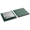
Analog to Digital Converters - ADC Single-channel, 9-bit, 1.3-GSPS analog-to-digital converter (ADC) with JESD204C interface 144-FCBGA -40 to 85 ADC09xJ1300 is a family of quad, dual and single channel, 9-bit, 1.3GSPS analog-to-digital converters (ADC). Low power consumption, high sampling rate and 9-bit resolution makes the ADC09xJ1300 ideally suited for suited for a variety of multi-channel communications and test systems. Full-power input bandwidth (-3dB) of 6GHz enables direct RF sampling of L-band and S-band. A number of clocking features are included to relax system hardware requirements, such as an internal phase-locked loop (PLL) with integrated voltagecontrolled oscillator (VCO) to generate the sampling clock. Four clock outputs are provided to clock the logic and SerDes of the FPGA or ASIC. A timestamp input and output is provided for pulsed systems. JESD204C serialized interface decreases system size by reducing the amount of printed circuit board (PCB) routing. Interface modes support from 2 to 8 lanes (dual and quad channel devices) or 1 to 4 lanes (for the single channel device), with SerDes baud-rates up to 17.16Gbps, to allow the optimal configuration for each application. Features • ADC Core: – Resolution: 9 Bit – Maximum sampling rate: 1.3GSPS – Non-interleaved architecture – Internal dither reduces high-order harmonics • Performance specifications (–1dBFS): – SNR (100 MHz): 53.5dBFS – ENOB (100 MHz): 8.5 Bits – SFDR (100 MHz): 64dBc – Noise floor (–20dBFS): –143dBFS • Full-scale input voltage: 80 mVPP-DIFF • Full-power input bandwidth: 6GHz • JESD204C Serial data interface: – Support for 2 to 8 (Quad/Dual channel) or 1 to 4 (Single channel) total SerDes lanes – Maximum baud-rate: 17.16Gbps – 64B/66B and 8B/10B encoding modes – Subclass-1 support for deterministic latency – Compatible with JESD204B receivers • Optional internal sampling clock generation – Internal PLL and VCO (7.2–8.2GHz) • SYSREF Windowing eases synchronization • Four clock outputs simplify system clocking – Reference clocks for FPGA or adjacent ADC – Reference clock for SerDes transceivers • Timestamp input and output for pulsed systems • Power consumption (1GSPS): – Quad Channel: 450mW / channel – Dual channel: 625mW / channel – Single channel: 940mW • Power supplies: 1.1V, 1.9V #CommonPartsLibrary #IntegratedCircuit #ADC #HighSpeedADC #RFADC #JESD204C #13GSPS #9bitADC #DirectRFSampling #TexasInstruments #MixedSignal #DataAcquisition #JESD204
0 Uses0 StarsXL6007E1
The XL6007 regulator is a wide input range, current mode, DC/DC converter which is capable of generating either positive or negative output voltages. It can be configured as either a boost, flyback, SEPIC or inverting converter. The XL6007 built in N-channel power MOSFET and fixed frequency oscillator, current-mode architecture results in stable operation over a wide range of supply and output voltages. The XL6007 regulator is special design for portable electronic equipment. Wide 3.6V to 24V Input Voltage Range Positive or Negative Output Voltage Programming with a Single Feedback Pin Current Mode Control Provides Excellent Transient Response 1.25V reference adjustable version Fixed 400KHz Switching Frequency Maximum 2A Switching Current SW PIN Built in Over Voltage Protection Excellent line and load regulation EN PIN TTL shutdown capability Internal Optimize Power MOSFET High efficiency up to 90% Built in Frequency Compensation Built in Soft-Start Function Built in Thermal Shutdown Function Built in Current Limit Function Available in SOP8 package Applications Automotive and Industrial Boost / Buck-Boost / Inverting Converters Portable Electronic Equipment #commonpartslibrary #integratedcircuit
0 Uses0 StarsADS1293CISQ/NOPB
3 Channel AFE 24 Bit 28-WQFN (5x5) ADS1293CISQ/NOPB is a highly integrated, low-power 3-channel ECG Analog Front-End (AFE) from Texas Instruments. It is designed for portable and battery-powered medical devices, fitness monitors, heart-rate monitoring systems, Holter monitors, and other electrocardiogram (ECG) applications. The device integrates signal acquisition, filtering, lead-off detection, right-leg drive generation, and high-resolution analog-to-digital conversion into a single IC, reducing external component count and system cost. Key Features Three high-resolution ECG acquisition channels 24-bit analog-to-digital conversion Simultaneous pace detection support Ultra-low power consumption of approximately 0.3 mW per channel Low input-referred noise of 7 µVpp (40 Hz bandwidth) Programmable sample rates up to 25.6 ksps Differential input voltage range of ±400 mV Integrated EMI-hardened input filters Flexible input routing matrix Built-in Right-Leg Drive (RLD) amplifier AC and DC lead-off detection Integrated Wilson and Goldberger terminal generation Battery voltage monitoring capability Internal oscillator and voltage reference ALARMB pin for interrupt-driven diagnostics and fault reporting Multiple power-down and standby modes for battery-powered systems SPI-compatible digital interface Operating temperature range: –20°C to +85°C 28-pin WQFN package (5 mm × 5 mm) Typical Applications Portable 1-, 3-, 5-, 6-, 7-, 8-, and 12-lead ECG systems Holter monitors Event recorders Telemedicine devices Patient vital-sign monitoring equipment Automated External Defibrillators (AEDs) Sports and fitness heart-rate monitors Wearable medical devices Hashtags #commonpartslibrary #integratedcircuit #TexasInstruments #ADS1293 #AFE #AnalogFrontEnd #ECG #Electrocardiogram #MedicalElectronics #HealthTech #WearableDevices #HeartRateMonitor #PatientMonitoring #BiomedicalEngineering #24BitADC #LowPowerDesign #SPI #SignalConditioning #PortableMedicalDevices #HolterMonitor #Telemedicine #VitalSignsMonitoring #EmbeddedSystems #MixedSignalIC #WQFN28 #BatteryPoweredDevices #MedicalInstrumentation
3 Uses0 Stars