Memory
A memory IC, or integrated circuit, is a type of electronic device that stores and retrieves data. It is used in a wide range of electronic devices, including computers, smartphones, and other electronic devices. Memory ICs come in a variety of types, including DRAM, SRAM, and Flash memory, and are used for different purposes depending on the device and application. One of the primary use cases for memory ICs is in computer systems, where they are used to store data and instructions that are accessed by the processor. Memory ICs are also used in a variety of other electronic devices, such as digital cameras, MP3 players, and mobile phones, to store data and enable various functions. Flux.ai has the world's largest community-driven public library of memory ICs, with a wide variety of footprints, symbols, datasheets, and simulation models available. This extensive library allows users to easily access and use memory ICs in their projects, making it an invaluable resource for engineers and developers.
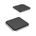
STM32F407VGT6
ARM Microcontrollers - MCU ARM M4 1024 FLASH 168 Mhz 192kB SRAM 100-LQFP (14x14) Arm® Cortex®-M4 32b MCU+FPU, 210DMIPS, up to 1MB Flash/192+4KB RAM, USB OTG HS/FS, Ethernet, 17 TIMs, 3 ADCs, 15 comm. interfaces & camera • Core: Arm® 32-bit Cortex®-M4 CPU with FPU, Adaptive real-time accelerator (ART Accelerator) allowing 0-wait state execution from Flash memory, frequency up to 168 MHz, memory protection unit, 210 DMIPS/ 1.25 DMIPS/MHz (Dhrystone 2.1), and DSP instructions • Memories – Up to 1 Mbyte of Flash memory – Up to 192+4 Kbytes of SRAM including 64- Kbyte of CCM (core coupled memory) data RAM – 512 bytes of OTP memory – Flexible static memory controller supporting Compact Flash, SRAM, PSRAM, NOR and NAND memories • LCD parallel interface, 8080/6800 modes • Clock, reset and supply management – 1.8 V to 3.6 V application supply and I/Os – POR, PDR, PVD and BOR – 4-to-26 MHz crystal oscillator – Internal 16 MHz factory-trimmed RC (1% accuracy) – 32 kHz oscillator for RTC with calibration – Internal 32 kHz RC with calibration • Low-power operation – Sleep, Stop and Standby modes –VBAT supply for RTC, 20×32 bit backup registers + optional 4 KB backup SRAM • 3×12-bit, 2.4 MSPS A/D converters: up to 24 channels and 7.2 MSPS in triple interleaved mode • 2×12-bit D/A converters • General-purpose DMA: 16-stream DMA controller with FIFOs and burst support • Up to 17 timers: up to twelve 16-bit and two 32- bit timers up to 168 MHz, each with up to 4 IC/OC/PWM or pulse counter and quadrature (incremental) encoder input • Debug mode – Serial wire debug (SWD) & JTAG interfaces – Cortex-M4 Embedded Trace Macrocell™ • Up to 140 I/O ports with interrupt capability – Up to 136 fast I/Os up to 84 MHz – Up to 138 5 V-tolerant I/Os • Up to 15 communication interfaces – Up to 3 × I2C interfaces (SMBus/PMBus) – Up to 4 USARTs/2 UARTs (10.5 Mbit/s, ISO 7816 interface, LIN, IrDA, modem control) – Up to 3 SPIs (42 Mbits/s), 2 with muxed full-duplex I2S to achieve audio class accuracy via internal audio PLL or external clock – 2 × CAN interfaces (2.0B Active) – SDIO interface • Advanced connectivity – USB 2.0 full-speed device/host/OTG controller with on-chip PHY – USB 2.0 high-speed/full-speed device/host/OTG controller with dedicated DMA, on-chip full-speed PHY and ULPI – 10/100 Ethernet MAC with dedicated DMA: supports IEEE 1588v2 hardware, MII/RMII #CommonPartsLibrary #IntegratedCircuit #Microcontroller #STM32F407
62 Uses0 StarsADXL345TCCZ-EP
Accelerometer X, Y, Z Axis ±2g, 4g, 8g, 16g 0.05Hz ~ 1.6kHz 14-LGA (3x5) The ADXL345-EP is an extended performance version of the ADXL345, which is a small, thin, ultralow power, 3-axis accelerometer with high resolution (13-bit) measurement at up to ±16 g. Digital output data is formatted as 16-bit twos complement and is accessible through either a SPI (3- or 4-wire) or I2 C digital interface. The ADXL345-EP is well suited for extended temperature range industrial and aerospace equipment. It measures the static acceleration of gravity in tilt-sensing applications, as well as dynamic acceleration resulting from motion or shock. Its high resolution (3.9 mg/LSB) enables measurement of inclination changes less than 1.0°. Several special sensing functions are provided. Activity and inactivity sensing detect the presence or lack of motion by comparing the acceleration on any axis with user-set thresholds. Tap sensing detects single and double taps in any direction. Freefall sensing detects if the device is falling. These functions can be mapped individually to either of two interrupt output pins. An integrated memory management system with a 32-level first in, first out (FIFO) buffer can be used to store data to minimize host processor activity and lower overall system power consumption. Low power modes enable intelligent motion-based power management with threshold sensing and active acceleration measurement at extremely low power dissipation. The ADXL345-EP is supplied in a small, thin, 3 mm × 5 mm × 1 mm, 14-lead, enhanced plastic package. Ultralow power: as low as 23 µA in measurement mode and 0.1 µA in standby mode at VS = 2.5 V (typical) Power consumption scales automatically with bandwidth User-selectable resolution from 10 to 13 bits 4 mg/LSB scale factor in all g ranges 32-sample FIFO minimizes host processor load Single tap, double tap, and free-fall detection Activity/inactivity monitoring Supply voltage range: 2.0 V to 3.6 V I/O voltage range: 1.7 V to VS SPI (3- and 4-wire) and I2C digital interfaces Flexible interrupt modes mappable to either interrupt pin Measurement ranges selectable via serial command Bandwidth selectable via serial command 10,000 g shock survival Pb free/RoHS compliant #commonpartslibrary #integratedcircuit #accelerometer
7 Uses0 StarsADXL345BCCZ
Accelerometer X, Y, Z Axis ±2g, 4g, 8g, 16g 0.05Hz ~ 1.6kHz 14-LGA (3x5) The ADXL345 is a small, thin, ultralow power, 3-axis accelerometer with high resolution (13-bit) measurement at up to ±16 g. Digital output data is formatted as 16-bit twos complement and is accessible through either a SPI (3- or 4-wire) or I2C digital interface. The ADXL345 is well suited for mobile device applications. It measures the static acceleration of gravity in tilt-sensing applications, as well as dynamic acceleration resulting from motion or shock. Its high resolution (3.9 mg/LSB) enables measurement of inclination changes less than 1.0°. Several special sensing functions are provided. Activity and inactivity sensing detect the presence or lack of motion by comparing the acceleration on any axis with user-set thresholds. Tap sensing detects single and double taps in any direction. Free-fall sensing detects if the device is falling. These functions can be mapped individually to either of two interrupt output pins. An integrated memory management system with a 32-level first in, first out (FIFO) buffer can be used to store data to minimize host processor activity and lower overall system power consumption. Low power modes enable intelligent motion-based power management with threshold sensing and active acceleration measurement at extremely low power dissipation. The ADXL345 is supplied in a small, thin, 3 mm × 5 mm × 1 mm, 14-lead, plastic package. ► Ultralow power: as low as 23 µA in measurement mode and 0.1 µA in standby mode at VS = 2.5 V (typical) ► Power consumption scales automatically with bandwidth ► User-selectable resolution ► Fixed 10-bit resolution ► Full resolution, where resolution increases with g range, up to 13-bit resolution at ±16 g (maintaining 4 mg/LSB scale factor in all g ranges) ► Embedded memory management system with FIFO technology minimizes host processor load ► Single tap/double tap detection ► Activity/inactivity monitoring ► Free-fall detection ► Supply voltage range: 2.0 V to 3.6 V ► I/O voltage range: 1.7 V to VS ► SPI (3- and 4-wire) and I2C digital interfaces ► Flexible interrupt modes mappable to either interrupt pin ► Measurement ranges selectable via serial command ► Bandwidth selectable via serial command ► Wide temperature range (−40°C to +85°C) ► 10,000 g shock survival ► Pb free/RoHS compliant #CommonPartsLibrary #IntegratedCircuit #Sensor #Transducer #Motion-Sensor #Accelerometer #ADXL345
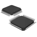
61 Uses0 StarsSTM32F103C8T6
ARM® Cortex® M3 STM32F1 Microcontroller IC 32-Bit Single-Core 72MHz 64KB (64K x 8) FLASH Medium-density performance line Arm®-based 32-bit MCU with 64 or 128 KB Flash, USB, CAN, 7 timers, 2 ADCs, 9 com. interfaces Arm® 32-bit Cortex®-M3 CPU core – 72 MHz maximum frequency, 1.25 DMIPS/MHz (Dhrystone 2.1) performance at 0 wait state memory access – Single-cycle multiplication and hardware division • Memories – 64 or 128 Kbytes of Flash memory – 20 Kbytes of SRAM • Clock, reset and supply management – 2.0 to 3.6 V application supply and I/Os – POR, PDR, and programmable voltage detector (PVD) – 4 to 16 MHz crystal oscillator – Internal 8 MHz factory-trimmed RC – Internal 40 kHz RC – PLL for CPU clock – 32 kHz oscillator for RTC with calibration • Low-power – Sleep, Stop and Standby modes – VBAT supply for RTC and backup registers • 2x 12-bit, 1 µs A/D converters (up to 16 channels) – Conversion range: 0 to 3.6 V – Dual-sample and hold capability – Temperature sensor • DMA – 7-channel DMA controller – Peripherals supported: timers, ADC, SPIs, I 2Cs and USARTs • Up to 80 fast I/O ports – 26/37/51/80 I/Os, all mappable on 16 external interrupt vectors and almost all 5 V-tolerant Debug mode: – Serial wire debug (SWD) and JTAG interfaces • Seven timers – Three 16-bit timers, each with up to 4 IC/OC/PWM or pulse counter and quadrature (incremental) encoder input – 16-bit, motor control PWM timer with dead-time generation and emergency stop – Two watchdog timers (independent and window) – SysTick timer 24-bit downcounter • Up to nine communication interfaces – Up to two I2C interfaces (SMBus/PMBus®) – Up to three USARTs (ISO 7816 interface, LIN, IrDA capability, modem control) – Up to two SPIs (18 Mbit/s) – CAN interface (2.0B Active) – USB 2.0 full-speed interface • CRC calculation unit, 96-bit unique ID • Packages are ECOPACK #commonpartslibrary #integratedcircuit #microcontroller #stm32f1
36 Uses0 StarsESP32-C6FH4
IC RF TxRx Only Bluetooth, WiFi Bluetooth v5.0, Thread, Zigbee® 2.412GHz ~ 2.484GHz 32-VFQFN Exposed Pad The ESP32-C6FH4 is a low-power, highly integrated wireless microcontroller from Espressif Systems, designed for IoT applications. It is based on a 32-bit RISC-V processor running at up to 160 MHz, providing efficient performance for embedded systems while maintaining low power consumption. This variant includes 4 MB of embedded flash memory, making it suitable for standalone applications without the need for external flash. The ESP32-C6FH4 supports multiple wireless communication protocols, including: Wi-Fi 6 (802.11ax) in the 2.4 GHz band (backward compatible with Wi-Fi 4/802.11 b/g/n) Bluetooth Low Energy (BLE 5) IEEE 802.15.4 (used for protocols like Thread and Zigbee) Key features include: Rich set of GPIO pins with support for peripherals such as UART, SPI, I2C, PWM, ADC, and more Integrated hardware security features (secure boot, flash encryption, cryptographic accelerators) Multiple low-power modes for battery-operated devices On-chip temperature sensor and RTC peripherals #commonpartslibrary #transceiver
62 Uses0 StarsAP510BFA-CBR
RF System on a Chip - SoC Cortex-M55 250MHz, 2.5D GPU, 4MB MRAM, 3.75MB SRAM, BLE5.4, -20 to +70 C, BGA , 1.71 V to 2.2 V -20C ~ 70C ARM® Cortex®-M55 System On Chip (SOC) IC Apollo510B 250MHz The AP510BFA-CBR is an ultra-low-power MCU System-on-Chip (SoC) designed for advanced embedded and edge-AI applications. It belongs to the Apollo510B series and integrates a powerful ARM Cortex-M55 processor optimized for both performance and energy efficiency. It combines processing, memory, and multiple peripherals into a single BGA package, making it suitable for compact and power-sensitive designs. Key Characteristics Core: ARM Cortex-M55 Max CPU Speed: 250 MHz Architecture: MCU / SoC Flash Memory: 4 MB RAM: ~3.75 MB Connectivity: I2C, SPI, UART, USB Wireless Support: Bluetooth 5.4 (variant dependent) Package: 153-BGA (compact high-density package) Key Features Built on Ambiq’s ultra-low-power SPOT technology Designed for battery-powered and energy-sensitive devices High computational performance for edge AI and DSP workloads Integrated peripherals for embedded system development Typical Applications Wearables (smartwatches, fitness bands) Smart home and IoT devices Edge AI / machine learning nodes Industrial sensors and monitoring systems Wireless communication modules #CommonPartsLibrary #IntegratedCircuit #SoC #Apollo510B
2 Uses0 StarsTC58NVG1S3HBAI6
NAND Flash 3.3V 2Gb 24nm SLC NAND (EEPROM) FLASH - NAND (SLC) Memory IC 2Gbit Parallel 25 ns 67-VFBGA (6.5x8) The TC58NVG1S3HBAI6 is a 2-Gbit (256M × 8) SLC NAND flash memory device originally developed by Toshiba (now Kioxia). It is a CMOS-based, electrically erasable and programmable read-only memory (EEPROM) used to store data even when power is removed. This device uses Single-Level Cell (SLC) NAND technology, which offers high reliability, fast access time, and long endurance, making it suitable for industrial and embedded systems. Key Characteristics Memory Type: NAND Flash (Non-volatile) Technology: SLC (Single-Level Cell) Density: 2 Gbit (256M × 8 organization) Interface: Parallel I/O Supply Voltage: 2.7 V – 3.6 V Access Time: ~25 ns Package: 67-ball VFBGA (compact surface-mount) Functional Overview Organized into pages and blocks (typical NAND structure) Supports operations such as: Read Page program (write) Block erase Copy-back operations Uses shared I/O pins for address, data, and command input/output Internally, data is transferred between the memory array and internal registers in page-sized chunks (~2176 bytes including spare area). Typical Applications Embedded systems storage Firmware and boot memory Industrial control systems Data logging devices Consumer electronics (e.g., cameras, audio storage) #CommonPartsLibrary #IntegratedCircuit #memory #TC58NVG1
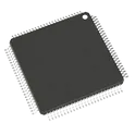
0 Uses0 StarsPIC32MZ2048EFM100-I/PT
MIPS32® M-Class PIC® 32MZ Microcontroller IC 32-Bit 200MHz 2MB (2M x 8) FLASH 100-TQFP (12x12) The PIC32MZ2048EFM100-I/PT is built around a MIPS32® M-Class core operating at up to 200 MHz, delivering high computational performance suitable for real-time control, signal processing, and communication-intensive systems. It integrates large on-chip memory, multiple communication interfaces, and rich peripheral support in a compact package. Key Features Core Architecture: 32-bit MIPS32® M-Class CPU Clock Speed: Up to 200 MHz Program Memory: 2 MB Flash RAM: 512 KB Package: 100-pin TQFP (12×12 mm), surface-mount Operating Voltage: 2.1 V to 3.6 V I/O Pins: Up to 78 programmable I/O Integrated Peripherals & Interfaces Communication Interfaces: CAN, Ethernet, USB OTG I²C, SPI, SQI, UART/USART Parallel Master Port (PMP) Analog Features: 40-channel, 12-bit ADC System Peripherals: DMA controller PWM modules Watchdog timer (WDT) Brown-out reset and power-on reset Advanced Features: Floating Point Unit (FPU) for fast math operations Hardware crypto engine (AES, SHA, etc., depending on variant) High-speed USB and Ethernet connectivity #CommonPartsLibrary #IntegratedCircuit #Microcontroller #PIC® 32MZ
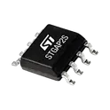
4 Uses0 StarsM24256E-FMN6TP
EEPROM Memory IC 256Kbit I2C 1 MHz 450 ns 8-SO The M24256E-FMN6TP is a 256-Kbit (32 Kbyte) I²C-compatible serial EEPROM from STMicroelectronics. It is designed for reliable, non-volatile data storage in a wide range of electronic applications including consumer, industrial, and automotive systems. The device supports standard (100 kHz), fast (400 kHz), and fast-mode plus (1 MHz) I²C communication, enabling efficient data transfer. It features byte and page write operations, low power consumption, and a high endurance of write cycles, making it suitable for frequent data logging and configuration storage. Housed in a compact SO8 package, the device is optimized for space-constrained PCB designs while maintaining robust performance and data retention capabilities. Key Features Memory size: 256 Kbit (32 Kbyte) Interface: I²C (2-wire serial interface) Clock frequency: Standard mode: 100 kHz Fast mode: 400 kHz Fast-mode Plus: 1 MHz Supply voltage range: 1.7 V to 5.5 V Page write capability: up to 64 bytes Write cycle time: ~5 ms (typical) Data retention: > 200 years Endurance: > 4 million write cycles Hardware write protection available ESD protection and latch-up immunity Functional Description The device operates as a slave on the I²C bus and supports: Byte write and read Page write (up to 64 bytes) Random and sequential read operations Memory addressing is internally managed using a 16-bit address pointer, allowing access to the full 32 KB memory array. The device includes an internal write cycle controller, eliminating the need for external timing management. Pin Configuration (SO8 Package) A0, A1, A2: Device address inputs VSS: Ground SDA: Serial data line SCL: Serial clock line WC: Write control (hardware write protection) VCC: Supply voltage Absolute Maximum Ratings Supply voltage (VCC): -0.3 V to 6.5 V Input voltage: -0.3 V to VCC + 0.6 V Storage temperature: -65°C to +150°C Operating temperature (industrial grade): -40°C to +85°C Electrical Characteristics Low standby current: < 1 µA (typical) Operating current: < 1 mA Input/output compatible with CMOS logic levels Schmitt trigger inputs for noise immunity Timing Characteristics Write cycle time: 5 ms (typical) Fast-mode Plus support up to 1 MHz Sequential read supports continuous data streaming Package Information Package type: SO8 (8-lead Small Outline) Mounting: Surface-mount (SMD) Tape & reel packaging (TP suffix) Applications Configuration storage Calibration data storage Data logging systems Industrial control systems Consumer electronics Embedded systems requiring non-volatile memory Advantages High endurance and long data retention Wide voltage range (ideal for mixed-voltage systems) Compact footprint High-speed I²C compatibility (up to 1 MHz) #commonpartslibrary #integratedcircuit #memory
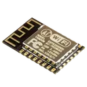
17 Uses0 StarsESP-12F
WiFi 802.11b/g/n Transceiver Module 2.4GHz ~ 2.5GHz Integrated, Trace Surface Mount The ESP-12F is a compact WiFi module based on the ESP8266EX, widely used in IoT and embedded systems due to its low cost and built-in networking capabilities. Integrated WiFi (2.4 GHz) Supports 802.11 b/g/n Built-in TCP/IP stack (no external WiFi processor needed) Microcontroller + WiFi in one Powered by the ESP8266EX SoC Can run user applications directly (not just a WiFi modem) Flash Memory Typically 4 MB SPI flash (varies by version) GPIO Support Multiple multifunction pins: Digital I/O PWM I2C SPI UART ADC (1 channel) Size: ~16 mm × 24 mm Mounting: Castellated SMD module Antenna: Built-in PCB trace antenna (requires proper keepout zone) Power Requirements Operating Voltage: 3.0V – 3.6V (typical 3.3V) Current Consumption: Idle: ~70 mA Peak (TX): up to ~300 mA Common Interfaces UART – programming and debugging SPI – peripheral communication I2C (software-based) GPIO – general-purpose control #commonpartslibrary #transceiver #module #wireless #rf #wifi
186 Uses0 Stars