Memory
A memory IC, or integrated circuit, is a type of electronic device that stores and retrieves data. It is used in a wide range of electronic devices, including computers, smartphones, and other electronic devices. Memory ICs come in a variety of types, including DRAM, SRAM, and Flash memory, and are used for different purposes depending on the device and application. One of the primary use cases for memory ICs is in computer systems, where they are used to store data and instructions that are accessed by the processor. Memory ICs are also used in a variety of other electronic devices, such as digital cameras, MP3 players, and mobile phones, to store data and enable various functions. Flux.ai has the world's largest community-driven public library of memory ICs, with a wide variety of footprints, symbols, datasheets, and simulation models available. This extensive library allows users to easily access and use memory ICs in their projects, making it an invaluable resource for engineers and developers.
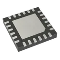
MAX17320G20+
Battery Fuel Gauge IC Lithium Ion/Polymer 24-TQFN (4x4) The MAX17320G20+ is a high-accuracy, ultra-low-power fuel gauge and battery protector IC designed for 2-cell to 4-cell lithium-ion and lithium-polymer battery packs. The device integrates Maxim Integrated’s ModelGauge™ m5 EZ algorithm to provide precise battery state-of-charge estimation without requiring battery relearning after system resets or battery replacement. It is optimized for portable, wearable, industrial, and IoT battery-powered applications where accurate battery monitoring and robust protection are required. The device combines fuel gauging, battery authentication support, autonomous battery protection, current sensing, and voltage monitoring into a single integrated solution. It includes configurable protection features such as overvoltage, undervoltage, overcurrent, short-circuit, and thermal protection, helping improve system safety and battery reliability. The MAX17320G20+ communicates through an I²C-compatible interface and supports low-power operation for extended battery runtime. Features High-accuracy battery fuel gauge for multi-cell lithium-ion batteries Supports 2-cell to 4-cell battery pack configurations Integrated ModelGauge m5 EZ algorithm with no battery relearning required Integrated battery protector with autonomous safety monitoring Supports overvoltage, undervoltage, overcurrent, short-circuit, and thermal protection Integrated current-sense amplifier for accurate current measurement Low quiescent current optimized for portable and always-on systems I²C-compatible communication interface Configurable alert and interrupt functions Battery aging compensation and cycle tracking Supports battery authentication functionality Integrated ADCs for voltage, current, and temperature monitoring Programmable protection thresholds and timing parameters Low-power hibernate and sleep operating modes Electrical Characteristics Designed for lithium-ion and lithium-polymer battery chemistries Supports battery stack voltages corresponding to 2S to 4S configurations High-resolution voltage, current, temperature, and capacity measurements Low operating current suitable for battery-powered systems Integrated precision coulomb counter Wide operating temperature range suitable for industrial applications Protection Functions Cell overvoltage protection Cell undervoltage protection Charge overcurrent protection Discharge overcurrent protection Short-circuit protection Overtemperature and undertemperature protection Permanent failure detection and fault logging Autonomous FET control for pack isolation Interface and Control I²C serial communication interface Programmable registers for protection and fuel gauge configuration Interrupt and alert outputs for fault and status indication Supports host processor communication and diagnostics Nonvolatile memory for configuration storage Package Information Package type is TQFN Compact surface-mount package suitable for space-constrained designs RoHS compliant and lead-free package option Typical Applications Smart battery packs Portable medical devices Industrial handheld equipment IoT and wireless sensor devices Battery-powered consumer electronics Portable test and measurement systems Rechargeable multi-cell battery systems #commonpartslibrary #integratedcircuit #powermanagement #batterymanagement
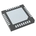
59 Uses0 StarsBQ41Z50RSNR
Battery Fuel Gauge IC Multi-Chemistry 32-QFN (4x4) The BQ41Z50RSNR is a highly integrated battery fuel gauge and battery management IC designed for single-cell and multi-cell lithium-ion and lithium-polymer battery packs. It provides accurate battery monitoring, protection, authentication, and state estimation functions for portable, industrial, and embedded power applications. The device incorporates advanced Impedance Track™ fuel gauging technology to deliver precise state-of-charge, state-of-health, and runtime predictions across varying operating conditions and battery aging profiles. The device integrates battery protection features including overvoltage, undervoltage, overcurrent, short-circuit, and temperature monitoring to enhance system safety and reliability. It supports SMBus and I²C communication interfaces for host processor interaction and system diagnostics. Internal flash memory allows programmable configuration parameters, calibration data, and battery profile storage. The BQ41Z50RSNR is optimized for compact battery-powered systems requiring accurate fuel gauging, low power consumption, and robust battery protection capabilities. Typical applications include notebooks, handheld devices, industrial instruments, portable medical equipment, smart battery packs, and embedded rechargeable systems. Engineering Specification Device Type Battery Fuel Gauge and Battery Management IC Battery Chemistry Support Lithium-Ion and Lithium-Polymer Cell Configuration Supports multi-cell battery pack configurations Fuel Gauging Technology Impedance Track™ battery fuel gauging Integrated Functions Battery monitoring State-of-charge estimation State-of-health estimation Remaining runtime prediction Battery protection Cell balancing support Authentication support Temperature monitoring Data logging and diagnostics Protection Features Overvoltage protection Undervoltage protection Overcurrent protection Short-circuit protection Charge and discharge protection Thermal protection Communication Interface SMBus compatible I²C compatible interface Non-Volatile Memory Integrated flash memory for configuration and battery profile storage Measurement Functions Battery voltage measurement Current measurement Temperature sensing Capacity tracking Cycle count monitoring Operating Voltage Designed for rechargeable battery pack applications Power Consumption Low-power operation optimized for portable devices Package Type QFN package Mounting Type Surface-mount device Operating Temperature Range Industrial operating temperature range suitable for portable and embedded applications Typical Applications Smart battery packs Portable electronics Industrial handheld equipment Medical portable devices Rechargeable embedded systems Battery-powered instrumentation #commonpartslibrary #integratedcircuit #powermanagement
0 Uses0 StarsSCD43-D-R2
Air Quality Sensor CO2 Sensor 2.5V/3.3V/5V 20-Pin SMD EP T/R The SCD41-D-R1 is a miniature photoacoustic carbon dioxide sensor module developed by Sensirion for high-accuracy environmental sensing applications. The device integrates a CO₂ sensing element, temperature sensor, humidity sensor, optical components, calibration memory, and digital signal processing into a compact surface-mount package suitable for embedded systems and portable electronics. The sensor utilizes photoacoustic sensing technology to provide precise carbon dioxide concentration measurements while maintaining low power consumption and long-term stability. Integrated humidity and temperature sensing capabilities enable environmental compensation and simplify system integration by reducing the need for external sensors. The SCD41 communicates through a standard I²C digital interface and supports automatic self-calibration functions for reliable long-term operation. Its compact footprint and low energy requirements make it suitable for battery-powered devices, smart building systems, HVAC equipment, indoor air quality monitoring systems, and IoT applications. The module is factory calibrated and designed for continuous monitoring of indoor air quality conditions. The integrated architecture minimizes external component requirements while enabling accurate sensing performance across a wide operating range. Key Features Photoacoustic CO₂ sensing technology Integrated temperature and humidity sensing High accuracy carbon dioxide measurement I²C digital communication interface Low power consumption operation Automatic self-calibration support Compact surface-mount package Factory calibrated output Long-term measurement stability Optimized for indoor air quality applications Low-profile PCB mounting design RoHS and halogen-free compliant Electrical Characteristics Low-voltage supply operation Low average current consumption suitable for portable devices Integrated digital signal processing Non-volatile calibration memory Standard I²C communication compatibility Stable operation across industrial environmental conditions Mechanical Characteristics Compact SMD package for space-constrained applications Surface-mount assembly compatible Low-profile package structure Integrated optical cavity and sensing chamber Moisture-sensitive device requiring controlled handling during assembly Functional Characteristics Real-time carbon dioxide concentration monitoring Simultaneous temperature and humidity measurement Automatic environmental compensation Continuous and periodic measurement modes Fast startup and measurement response Long operational lifetime with stable calibration Optimized airflow design for accurate sensing Suitable for continuous indoor environmental monitoring Typical Applications Indoor air quality monitoring systems Smart thermostats and HVAC controllers Building automation equipment Demand-controlled ventilation systems Portable environmental monitoring devices Smart home and IoT products Air purification systems Occupancy and ventilation monitoring Battery-powered sensing devices Consumer and industrial environmental monitoring equipment #commonpartslibrary #sensor #airquality
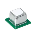
4 Uses0 StarsSCD41-D-R1
Air Quality Sensor CO2 Sensor 2.5V/3.3V/5V 20-Pin SMD EP T/R The SCD41-D-R1 is a miniature photoacoustic carbon dioxide sensor module developed by Sensirion for high-accuracy environmental sensing applications. The device integrates a CO₂ sensing element, temperature sensor, humidity sensor, optical components, calibration memory, and digital signal processing into a compact surface-mount package suitable for embedded systems and portable electronics. The sensor utilizes photoacoustic sensing technology to provide precise carbon dioxide concentration measurements while maintaining low power consumption and long-term stability. Integrated humidity and temperature sensing capabilities enable environmental compensation and simplify system integration by reducing the need for external sensors. The SCD41 communicates through a standard I²C digital interface and supports automatic self-calibration functions for reliable long-term operation. Its compact footprint and low energy requirements make it suitable for battery-powered devices, smart building systems, HVAC equipment, indoor air quality monitoring systems, and IoT applications. The module is factory calibrated and designed for continuous monitoring of indoor air quality conditions. The integrated architecture minimizes external component requirements while enabling accurate sensing performance across a wide operating range. Key Features Photoacoustic CO₂ sensing technology Integrated temperature and humidity sensing High accuracy carbon dioxide measurement I²C digital communication interface Low power consumption operation Automatic self-calibration support Compact surface-mount package Factory calibrated output Long-term measurement stability Optimized for indoor air quality applications Low-profile PCB mounting design RoHS and halogen-free compliant Electrical Characteristics Low-voltage supply operation Low average current consumption suitable for portable devices Integrated digital signal processing Non-volatile calibration memory Standard I²C communication compatibility Stable operation across industrial environmental conditions Mechanical Characteristics Compact SMD package for space-constrained applications Surface-mount assembly compatible Low-profile package structure Integrated optical cavity and sensing chamber Moisture-sensitive device requiring controlled handling during assembly Functional Characteristics Real-time carbon dioxide concentration monitoring Simultaneous temperature and humidity measurement Automatic environmental compensation Continuous and periodic measurement modes Fast startup and measurement response Long operational lifetime with stable calibration Optimized airflow design for accurate sensing Suitable for continuous indoor environmental monitoring Typical Applications Indoor air quality monitoring systems Smart thermostats and HVAC controllers Building automation equipment Demand-controlled ventilation systems Portable environmental monitoring devices Smart home and IoT products Air purification systems Occupancy and ventilation monitoring Battery-powered sensing devices Consumer and industrial environmental monitoring equipment #commonpartslibrary #sensor #airquality
615 Uses0 StarsTMP114NCIYMTR
Temperature Sensor Digital, Local -40°C ~ 125°C 16 b 4-PICOSTAR (0.76x0.76) The TMP114NCIYMTR is a high-accuracy digital temperature sensor designed for precision thermal monitoring applications in industrial, automotive, medical, and embedded electronic systems. The device integrates a precision band-gap temperature sensing element, analog-to-digital conversion circuitry, EEPROM memory, and a digital communication interface within a compact low-power package. The sensor supports accurate local temperature measurements with factory calibration and programmable alert functionality, enabling reliable thermal protection and environmental monitoring in space-constrained designs. Engineering Specification Manufacturer: Texas Instruments Manufacturer Part Number: TMP114NCIYMTR Device Type: Digital Temperature Sensor Temperature Measurement Method: Local Semiconductor Temperature Sensing Interface Type: I²C-Compatible Serial Interface Supply Voltage Range: Ultra-Low Voltage Operation Compatible with Battery-Powered Systems Temperature Measurement Range: Industrial Temperature Range Support Accuracy: High-Precision Factory-Calibrated Temperature Measurement Resolution: High-Resolution Digital Temperature Output Conversion Architecture: Integrated Sigma-Delta Analog-to-Digital Conversion Programmable Features: High and low temperature alert thresholds EEPROM-stored configuration settings Programmable conversion rate Offset correction calibration Alert and interrupt functionality Power Consumption: Optimized for Low-Power Embedded Applications Communication Speed: Standard and Fast-Mode I²C Support Package Type: Small Outline Leadless Package Mounting Type: Surface Mount Technology Operating Environment: Suitable for Industrial and Embedded Control Systems Protection Features: Integrated thermal monitoring alerts Nonvolatile configuration retention Robust digital communication interface Applications: Industrial temperature monitoring Medical instrumentation Battery-powered electronics Thermal management systems Precision embedded sensing Data acquisition equipment Environmental monitoring devices #commonpartslibrary #integratedcircuit #temperaturesensor #digital
5 Uses0 StarsBQ27220YZFR
Battery Battery Monitor IC Lithium Ion 9-DSBGA The BQ27220YZFR is a highly integrated single-cell battery fuel gauge IC developed for rechargeable lithium-ion and lithium-polymer battery applications. The device utilizes Texas Instruments’ Impedance Track™ algorithm to provide highly accurate battery capacity measurement, state-of-charge estimation, runtime prediction, and battery health monitoring across varying load and temperature conditions. The device is designed for compact portable electronics, wearable devices, IoT products, handheld instruments, and low-power embedded systems requiring precise battery monitoring and extended operating life. The BQ27220YZFR supports system-side fuel gauging without requiring battery pack-side electronics, simplifying battery integration and reducing overall system cost. The fuel gauge continuously monitors battery voltage, current, and temperature to estimate available capacity, remaining runtime, full charge capacity, and state-of-health information. Integrated low-power operation enables ultra-low standby current consumption suitable for always-on battery-powered products. Communication with the host processor is implemented through a standard I²C interface, allowing configuration access, telemetry reporting, and battery parameter monitoring. The device also integrates protection and alert functionality through programmable interrupt outputs and battery condition monitoring features. The BQ27220YZFR is optimized for use with single-cell lithium-based chemistries and supports learning cycles for adaptive battery characterization over product lifetime. Internal data flash memory stores battery profile information and calibration parameters to improve long-term gauging accuracy. The device is supplied in a compact lead-free wafer chip-scale package suitable for space-constrained PCB designs and portable electronics requiring minimal footprint and low-profile assembly. Electrical Characteristics Device Type Single-cell battery fuel gauge and battery monitor IC Battery Chemistry Support Lithium-ion and lithium-polymer rechargeable batteries Input Voltage Range Supports single-cell battery operation Fuel Gauging Method Impedance Track™ algorithm Communication Interface I²C serial interface Measurement Functions Battery voltage monitoring Battery current monitoring Battery temperature monitoring State-of-charge estimation Remaining capacity calculation Full charge capacity estimation State-of-health reporting Runtime prediction Power Consumption Ultra-low operating current for portable applications Temperature Monitoring External thermistor support Host Alert Features Interrupt and alert reporting capability Data Storage Integrated nonvolatile configuration memory Calibration Features Automatic learning and battery characterization support Protection Monitoring Battery condition and system monitoring functions Package Type DSBGA wafer chip-scale package Mounting Style Surface mount Operating Temperature Range Industrial temperature operation suitable for portable electronics Functional Features High-accuracy fuel gauging over battery lifetime Adaptive battery modeling and aging compensation Low-power operation for battery-powered systems Integrated battery profiling capability Real-time remaining runtime estimation Automatic battery learning cycles Compact PCB footprint for portable devices System-side implementation without smart battery pack requirement Programmable battery alert functionality Support for low-power embedded processors and mobile systems Optimized for wearable and IoT applications RoHS compliant and lead-free package construction #commonpartslibrary #integratedcircuit #powermanagement #batterymanagement
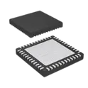
31 Uses0 StarsNRF52840-QFAA-F-R
IC RF TxRx + MCU 802.15.4, Bluetooth Bluetooth v5.0, Thread, Zigbee® 2.4GHz 48-VFQFN Exposed Pad The NRF52840-QFAA-F-R belongs to Nordic’s nRF52 series and supports multiple wireless standards including Bluetooth 5, Bluetooth Low Energy (BLE), Thread, Zigbee, ANT, and proprietary 2.4 GHz protocols. It features a 64 MHz ARM Cortex-M4F CPU with floating-point unit (FPU), making it suitable for both wireless communication and real-time embedded processing. The device integrates large memory resources, rich peripherals, USB support, NFC capability, and advanced security features, reducing the need for external components in wireless embedded designs. Key Features 32-bit ARM Cortex-M4F processor running at 64 MHz 1 MB Flash memory and 256 KB RAM Supports Bluetooth 5 / BLE, Thread, Zigbee, ANT, and proprietary 2.4 GHz protocols IEEE 802.15.4 compliant radio Up to +8 dBm TX output power High receiver sensitivity down to −103 dBm Data rates up to 2 Mbps Ultra-low power consumption for battery-powered applications USB 2.0 Full-Speed controller NFC-A tag support Multiple communication interfaces: SPI UART I2C (TWI) I2S PWM PDM ADC Up to 48 GPIOs Integrated ARM CryptoCell-310 security engine Operating voltage range: 1.7 V to 5.5 V Operating temperature: −40°C to +85°C Compact 48-QFN (6×6 mm) package Typical Applications BLE devices Smart home products Wearables Wireless sensors Industrial IoT HID devices (keyboard/mouse) Asset tracking Mesh networking devices USB dongles and gateways PCB Design Notes Community PCB reviews commonly recommend: Proper RF grounding and 50-ohm antenna routing Using ESD/TVS protection on USB lines Keeping RF matching components close to the antenna Using solid ground planes for 2.4 GHz performance #CommonPartsLibrary #IntegratedCircuit #RF
28 Uses0 StarsSTM32U3C5JIY6QTR
Ultra-low-power Arm® Cortex®-M33 32-bit MCU+TrustZone®+FPU, 395 CoreMark®, 2 MB flash memory, 640 KB SRAM, SMPS, crypto • 1.71 V to 3.6 V power supply • -40 °C to +105 °C temperature range • VBAT mode: supply for RTC, 32 x 32-bit backup registers • 1.6 μA Stop 3 mode with 8-Kbyte SRAM • 3.15 μA Stop 3 mode with full SRAM • 3.5 μA Stop 2 mode with 8-Kbyte SRAM • 5.7 μA Stop 2 mode with full SRAM • 12 μA/MHz Run mode @ 3.3 V, 48 MHz (While(1) SMPS step-down converter mode) • 15.5 μA/MHz Run mode @ 3.3 V, 48 MHz (CoreMark® SMPS step-down converter mode) • 20 μA/MHz Run mode @ 3.3 V, 96 MHz (CoreMark® SMPS step-down converter mode) • Brownout reset (BOR) in all modes except Shutdown mode Arm® 32-bit Cortex®-M33 CPU with TrustZone® and FPU ART Accelerator • 8-Kbyte instruction cache allowing 0-wait-state execution from flash and external memories: frequency up to 96 MHz, MPU, 144 DMIPS and DSP #CommonPartsLibrary #IntegratedCircuit
11 Uses0 StarsEFR32ZG23B020F512IM48-B
IC RF TxRx + MCU General ISM < 1GHz Z-Wave® 863MHz ~ 870MHz, 902MHz ~ 928MHz 48-VFQFN Exposed Pad The Silicon Labs EFR32ZG23B020F512IM48-B is a 2.4 GHz–independent (sub-GHz) RF Tx/Rx + MCU SoC optimized for Z-Wave smart home and IoT mesh networks. It integrates computing, RF communication, and security features in a compact 48-pin QFN package. It is part of the EFR32ZG23 Series 2 platform, which focuses on low-power, secure, long-range wireless connectivity for smart home, building automation, and industrial IoT devices. Key Features MCU Core & Memory ARM Cortex-M33 core (up to ~80 MHz) 512 kB Flash memory 64 kB RAM RF / Wireless Z-Wave protocol support (mesh + long-range) Frequency bands: 863–870 MHz (EU) 902–928 MHz (US) Max data rate: up to 100 kbps Output power: up to +20 dBm High sensitivity: around –110 dBm Security Secure Vault™ high-level security subsystem Hardware cryptography support Secure boot and key protection (IoT-grade security) Low Power Performance Ultra-low receive and transmit currents (single-digit mA RX, tens of mA TX) Designed for battery-powered IoT nodes Peripherals & Interfaces GPIO (up to ~31 pins depending on variant) ADC, I2C, SPI, UART, I2S, IrDA Flexible digital/analog peripheral integration Package & Electrical 48-pin QFN (6 × 6 mm) Supply voltage: 1.71 V – 3.8 V Industrial temperature range: –40°C to +125°C #CommonPartsLibrary #IntegratedCircuit #RF-transceiver #EFR32ZG23B020
0 Uses0 StarsdsPIC33CK256MP205-I/M4
dsPIC dsPIC™ 33CK, Functional Safety (FuSa) Microcontroller IC 16-Bit 100MHz 256KB (256K x 8) FLASH 48-UQFN (6x6) 28/36/48/64/80-Pin Digital Signal Controllers with High-Resolution PWM and CAN Flexible Data (CAN FD) Operating Conditions • 3.0V to 3.6V, -40°C to +125°C, DC to 100 MIPS • 3.0V to 3.6V, -40°C to +150°C, DC to 70 MIPS Core: 16-Bit dsPIC33CK CPU • 32-256 Kbytes of Program Flash with ECC and 8-24K RAM • Fast 6-Cycle Divide • LiveUpdate • Code Efficient (C and Assembly) Architecture • 40-Bit Wide Accumulators • Single-Cycle (MAC/MPY) with Dual Data Fetch • Single-Cycle, Mixed-Sign MUL Plus Hardware Divide • 32-Bit Multiply Support • Four Sets of Interrupt Context Saving Registers which Include Accumulator and STATUS for Fast Interrupt Handling • Zero Overhead Looping • RAM Memory Built-In Self-Test (MBIST) Clock Management • Internal Oscillator • Programmable PLLs and Oscillator Clock Sources • Reference Clock Output • Fail-Safe Clock Monitor (FSCM) • Fast Wake-up and Start-up • Backup Internal Oscillator Power Management • Low-Power Management Modes (Sleep, Idle, Doze) • Integrated Power-on Reset and Brown-out Reset High-Speed PWM • Eight PWM Pairs • Up to 250 ps PWM Resolution • Dead Time for Rising and Falling Edges • Dead-Time Compensation • Clock Chopping for High-Frequency Operation • PWM Support for: - DC/DC, AC/DC, inverters, PFC, lighting - BLDC, PMSM, ACIM, SRM motors • Fault and Current Limit Inputs • Flexible Trigger Configuration for ADC Triggering Timers/Output Compare/Input Capture • One General Purpose Timer • Peripheral Trigger Generator (PTG): - Up to 15 trigger sources to other peripheral modules - CPU independent state machine-based instruction sequencer • Nine MCCP/SCCP modules which Include Timer, Capture/Compare and PWM: - One MCCP - Eight SCCPs - 16 or 32-bit time base - 16 or 32-bit capture - 4-deep capture buffer • Fully Asynchronous Operation, Available in Sleep Modes #CommonPartsLibrary #IntegratedCircuit #Microcontroller #DSPIC33CK256MP
10 Uses0 Stars