Memory
A memory IC, or integrated circuit, is a type of electronic device that stores and retrieves data. It is used in a wide range of electronic devices, including computers, smartphones, and other electronic devices. Memory ICs come in a variety of types, including DRAM, SRAM, and Flash memory, and are used for different purposes depending on the device and application. One of the primary use cases for memory ICs is in computer systems, where they are used to store data and instructions that are accessed by the processor. Memory ICs are also used in a variety of other electronic devices, such as digital cameras, MP3 players, and mobile phones, to store data and enable various functions. Flux.ai has the world's largest community-driven public library of memory ICs, with a wide variety of footprints, symbols, datasheets, and simulation models available. This extensive library allows users to easily access and use memory ICs in their projects, making it an invaluable resource for engineers and developers.
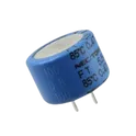
FT0H474ZF
470 mF (EDLC) Supercapacitor 5.5 V Radial, Can 6.5Ohm @ 1kHz The FT0H474ZF is a 5.5 V electric double-layer capacitor (EDLC), also known as a supercapacitor, manufactured by KEMET. It provides 470 mF (0.47 F) of capacitance for energy storage, backup power, and short-duration power hold-up applications. Designed for through-hole mounting in a radial can package, it offers high reliability, a wide operating temperature range, and long cycle life, making it suitable for memory backup, RTC backup, industrial electronics, and low-power energy storage systems. Key Features 470 mF (0.47 F) capacitance 5.5 V rated voltage Electric Double-Layer Capacitor (EDLC) technology Radial through-hole package Long operational life with excellent charge/discharge cycle capability Wide operating temperature range: −40°C to +85°C Low maintenance energy storage solution Suitable for backup power, memory retention, and peak power assistance RoHS compliant Reliable performance for industrial and consumer electronic applications #KEMET #Supercapacitor #EDLC #EnergyStorage #BackupPower #MemoryBackup #PowerHoldUp #RadialCapacitor #ThroughHole #Electronics #IndustrialElectronics #LowPowerDesign #CommonPartsLibrary #Capacitor
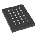
0 Uses0 StarsIS66WVH64M8DBLL-166B1LI
PSRAM (Pseudo SRAM) Memory IC 512Mbit HyperBus 166 MHz 36 ns 24-TFBGA (6x8) The IS66/67WVH64M8DALL/BLL are 512Mb Dual Die device containing two units of 256Mbit Pseudo Static Random Access Memory, organized as 64M words by 8 bits. The device supports a HyperBus interface, Very Low Signal Count (Address, Command and data through 8 DQ pins), Hidden Refresh Operation, and Automotive Temperature Operation, designed especially for Mobile and Automotive applications Key Features 512-Mbit (64M × 8) HyperRAM™ PSRAM High-speed HyperBus interface Clock frequency up to 166 MHz Fast 36 ns access time Single-ended clock architecture with reduced pin count Operating voltage range: 2.7 V to 3.6 V Industrial temperature range: −40°C to +85°C Low-power volatile memory solution Surface-mount 24-TFBGA (6 mm × 8 mm) package Suitable for graphics, AI edge devices, networking, and embedded systems requiring large external memory capacity. #CommonPartsLibrary #IntegratedCircuit #HyperRAM #PSRAM #ISSI #MemoryIC #HyperBus #EmbeddedSystems #IndustrialElectronics #IoT #HighSpeedMemory #BGA #VolatileMemory #EdgeComputing #HMI #ElectronicsDesign
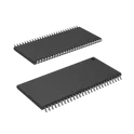
2 Uses0 StarsAS4C32M16SB-7TCN
SDRAM Memory IC 512Mbit Parallel 143 MHz 5.4 ns 54-TSOP II The AS4C32M16SB-7TCN is a single-data-rate synchronous dynamic random-access memory (SDR SDRAM) device manufactured by Alliance Memory. It is organized internally as a multi-bank array, allowing concurrent access operations across banks to improve effective memory bandwidth compared to simpler asynchronous DRAM architectures. The device is intended for general-purpose embedded memory applications where a synchronous, clock-driven memory interface is required, including embedded systems, industrial controllers, consumer electronics, networking equipment, and other designs that rely on a parallel SDRAM interface for working memory or buffering. As a drop-in style component within Alliance Memory's broader memory portfolio, this part is designed to be pin- and function-compatible with legacy SDR SDRAM devices originally offered by other manufacturers, allowing designers to source a continued-availability alternative for designs that depend on this memory architecture even as some original suppliers have discontinued production. This makes the device particularly useful in long-lifecycle industrial, embedded, and legacy system designs where a guaranteed supply of a specific memory interface and timing profile is critical to sustaining production over many years. The "B" designation in the part family indicates a specific die revision within the AS4C32M16S product line, reflecting a particular generation of internal silicon design while maintaining functional and pinout compatibility with related die revisions in the same footprint. The device communicates over a standard synchronous SDRAM command interface, using a clock-synchronized protocol for row and column addressing, data burst transfers, and bank management, and it supports the auto-refresh and self-refresh mechanisms typical of SDRAM devices to maintain stored data integrity without requiring constant external refresh management by the host controller. Mechanically, the device is housed in a thin small-outline package suited to space-constrained PCB layouts, and it is built for standard surface-mount assembly processes. The "-7TCN" suffix on this part number reflects a specific speed grade, package style, and temperature grade combination within the product family, with this particular variant intended for commercial temperature range operation. The device is supplied in tray packaging for surface-mount assembly and is compliant with RoHS material restrictions, supporting standard environmental and regulatory requirements for electronic components. Spec Sheet Identification Part Number: AS4C32M16SB-7TCN Device Family: AS4C32M16SB Manufacturer: Alliance Memory, Inc. Die Revision: B-die Functional Classification Device Type: Synchronous DRAM (SDR SDRAM) Memory Organization: Multi-bank array architecture Interface Type: Parallel, clock-synchronous command interface Refresh Capability: Supports auto-refresh and self-refresh modes Electrical Characteristics Supply Voltage: Standard 3.3V-class SDRAM supply rating Clock Frequency: Mid-range SDR SDRAM clock speed class Access Timing: Standard SDR SDRAM access time class for its speed grade Environmental & Qualification Temperature Grade: Commercial ("C" suffix designation) RoHS Compliance: Yes Product Positioning: Long-lifecycle, drop-in replacement memory device Package Package Type: Thin Small Outline Package, TSOP-II style Mounting: Surface mount technology (SMT) Packaging Format Supply Format: Tray packaging #AS4C32M16SB #AllianceMemory #SDRAM #SDRSDRAM #MemoryIC #EmbeddedMemory #TSOP #SurfaceMount #LegacyMemory #DropInReplacement #DRAM #EmbeddedSystems #IndustrialElectronics #SemiconductorIC #EngineeringSpec #ComponentLibrary #CommonPartsLibrary #RoHSCompliant #MemoryComponent #PCBDesign #CommonPartsLibrary #IntegratedCircuit #Memory #AS4C32
15 Uses0 StarsIRLR7843TRPBF
N-Channel 30 V 161A (Tc) 140W (Tc) Surface Mount TO-252AA (DPAK) The IRLR7843TRPBF is an N-channel power MOSFET built on Infineon's HEXFET technology platform, originally developed by International Rectifier. It is designed as a low-voltage, high-current switching device intended for applications where minimizing conduction loss and maximizing efficiency are primary design goals. The part is particularly well suited to synchronous switching topologies, where pairs or arrays of MOSFETs alternately conduct to regulate power flow with minimal energy dissipation. This device targets high-density power conversion applications where board space is limited but current demands are substantial, such as notebook computer power delivery, point-of-load converters used in servers, and advanced telecom and datacom equipment. It is commonly found supporting synchronous buck converter stages that step down a higher input rail to a lower output voltage suitable for powering processors, memory, and other low-voltage digital logic. Its low on-resistance characteristic allows it to carry significant current while generating comparatively little resistive heating, which is essential in compact enclosures with constrained thermal budgets. The transistor is fabricated using a refined trench gate process that improves upon earlier HEXFET generations, offering reduced gate charge and lower switching losses alongside its low conduction resistance. This combination makes it effective in both the high-side and low-side positions of a synchronous switching cell, where fast, clean transitions reduce overlap losses and improve overall converter efficiency. The device also offers well-characterized avalanche energy ratings, giving designers confidence in its ruggedness when exposed to transient overvoltage events that can occur during switching, and it presents a very low gate impedance, allowing it to be driven efficiently by standard gate driver circuitry. Mechanically, the part is housed in a surface-mount power package with an exposed tab for enhanced thermal conduction to the host PCB, allowing heat generated during operation to be efficiently transferred away from the silicon die. This package style is widely used in power-dense designs where through-hole packages would be impractical. The device is supplied in a tape-and-reel format suitable for automated assembly and is compliant with RoHS material restrictions, reflecting current environmental and regulatory standards for electronic components. Spec Sheet Identification Part Number: IRLR7843TRPBF Device Family: HEXFET Power MOSFET Manufacturer: Infineon Technologies Functional Classification Device Type: Power MOSFET Channel Type: N-channel Technology: Trench-gate HEXFET (IR MOSFET legacy technology) Logic Level Compatibility: Logic-level gate drive compatible Electrical Characteristics Drain-to-Source Voltage Rating: Low-voltage class, optimized for sub-30V rail applications On-Resistance: Ultra-low on-resistance class Drain Current Capability: High continuous current class Gate Charge: Low gate charge, optimized for fast switching Gate Impedance: Ultra-low gate impedance Avalanche Characteristics: Fully characterized avalanche voltage and current rating Switching & Application Behavior Primary Application: Synchronous buck converter switching stages Suitable Position: High-side and low-side switch positions Target Use Cases: Point-of-load conversion, notebook power delivery, telecom/datacom power systems Thermal & Mechanical Package Type: Surface-mount power package with exposed thermal tab (DPAK-style) Mounting: Surface mount technology (SMT) Thermal Path: Tab-based conduction to PCB for heat dissipation Environmental & Qualification RoHS Compliance: Yes Lifecycle Status: Active production Packaging Format Supply Format: Tape-and-reel, per part suffix designation #IRLR7843 #Infineon #HEXFET #PowerMOSFET #NChannelMOSFET #SynchronousBuck #PowerElectronics #DCDCConverter #PointOfLoad #PowerConversion #DPAK #SMTPackage #RoHSCompliant #SemiconductorIC #EngineeringSpec #ComponentLibrary #CommonPartsLibrary #PowerDensity #LowRDSon #DiscreteSemiconductor #commonpartslibrary #transistor
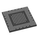
3 Uses0 StarsSTM32MP157CAC3
ARM® Cortex®-A7 Microprocessor IC STM32MP1 2 Core, 32-Bit 209MHz, 650MHz 361-TFBGA (12x12) # Engineering Specification ## Product Name STM32MP157CAC3 ## General Description STM32MP157CAC3 is a high-performance microprocessor unit that combines application processing and real-time control capabilities within a single integrated circuit. The device is designed to support advanced embedded systems requiring a balance of computing performance, deterministic control, multimedia processing, connectivity, and security functionality. The component integrates multi-core processing resources, memory interfaces, graphics capabilities, peripheral controllers, and communication subsystems to enable the development of sophisticated embedded platforms. Its heterogeneous architecture allows high-level operating systems and real-time firmware to operate simultaneously, supporting applications that require both user-interface functionality and low-latency control. The device is intended for industrial automation, human-machine interface systems, edge computing platforms, communication equipment, medical devices, smart infrastructure, and Internet of Things applications. Its architecture enables consolidation of system functions, reducing component count and simplifying overall hardware design. The design emphasizes processing efficiency, system scalability, power management, security, and long-term reliability. It supports advanced software ecosystems and facilitates the development of connected embedded products with graphical interfaces, networking capabilities, and real-time operational control. ## Functional Requirements ### Application Processing The device shall provide application-level processing capabilities suitable for operating systems, middleware, and user applications. ### Real-Time Processing The device shall support deterministic control functions for time-critical embedded operations. ### Multimedia Support The component shall support graphical and multimedia processing functions for display and user-interface applications. ### System Integration The device shall integrate processing, communication, and peripheral functions within a unified embedded computing platform. ## Electrical Requirements ### Power Management The device shall support efficient power operation and multiple power management modes to optimize energy consumption. ### Memory Interface Support The component shall support external memory devices for program execution, data storage, and system operation. ### Peripheral Connectivity The device shall provide interfaces for communication, control, monitoring, and external subsystem integration. ### Signal Integrity The design shall support reliable operation across supported interface standards and operating conditions. ## Processing Architecture Requirements ### Multi-Core Operation The device shall support concurrent execution of application and real-time workloads through integrated processing resources. ### Operating System Support The architecture shall support embedded operating systems and software frameworks suitable for advanced application development. ### Security Features The device shall support hardware-based mechanisms intended to protect system integrity, software assets, and sensitive data. ### Resource Management The component shall support efficient allocation of processing, memory, and peripheral resources. ## Mechanical Requirements ### Surface Mount Construction The device shall be supplied in a high-density surface mount package suitable for automated manufacturing processes. ### PCB Integration The package shall support integration into multilayer printed circuit boards designed for high-performance embedded systems. ### Structural Integrity The device shall maintain electrical and mechanical reliability during assembly and operational service life. ## Environmental Requirements ### Operating Conditions The component shall operate reliably within environmental conditions commonly encountered in industrial and embedded applications. ### Thermal Performance The device shall support stable operation under sustained processing workloads and associated thermal conditions. ### Storage and Handling The component shall maintain physical and electrical integrity during transportation, storage, and manufacturing processes. ## Quality Requirements ### Reliability The device shall provide dependable long-term operation in embedded and industrial computing environments. ### Verification Processing, peripheral, communication, and system functions shall be validated through applicable testing and qualification procedures. ### Compliance The product shall conform to relevant semiconductor, quality, and embedded computing standards applicable to its intended use. ## Documentation Requirements Technical documentation shall include processor architecture information, hardware integration guidelines, memory interface recommendations, power management considerations, software development support, security features, and application design guidance. ## Classification Tags #STM32MP157CAC3 #STM32MP1 #Microprocessor #MPU #EmbeddedProcessor #ARMProcessor #EmbeddedLinux #RealTimeControl #IndustrialAutomation #HumanMachineInterface #EdgeComputing #IoTGateway #EmbeddedSystems #SystemOnChip #SoC #ApplicationProcessor #GraphicsProcessor #ConnectivityPlatform #IndustrialElectronics #PCBDesign #HardwareDevelopment #ElectricalEngineering #CommonPartsLibrary #ComponentLibrary #EngineeringSpecification #TechnicalDocumentation #SystemIntegration #SecureEmbeddedSystems #MulticoreProcessing
9 Uses0 StarsMCP4461-103E/ST
Digital Potentiometer 10k Ohm 4 Circuit 257 Taps I2C Interface 20-TSSOP # Engineering Specification ## Product Name MCP4461-103E/ST ## General Description MCP4461-103E/ST is a non-volatile digital potentiometer integrated circuit designed to provide electronically programmable resistance adjustment for analog and mixed-signal applications. The device enables precise digital control of resistance values through a serial communication interface, eliminating the need for manual potentiometer adjustments and enhancing system automation capabilities. The component integrates multiple resistor networks, non-volatile memory, and digital control logic within a compact package, making it suitable for signal conditioning, gain adjustment, calibration, offset trimming, volume control, and configuration management applications. The design supports reliable operation in embedded systems, industrial electronics, instrumentation equipment, communication devices, and consumer products requiring programmable analog control. The device is optimized for ease of integration, low power consumption, repeatable performance, and long-term reliability. Non-volatile memory functionality allows resistance settings to be retained during power interruptions, supporting consistent system behavior and simplified startup configuration. ## Functional Requirements ### Digital Resistance Control The device shall provide programmable resistance adjustment through a digital communication interface. ### Non-Volatile Memory Operation The device shall retain programmed resistance settings when power is removed and restore stored values upon power-up. ### Multi-Channel Adjustment The device shall support independent control of multiple resistance channels for flexible system configuration. ### Analog Signal Conditioning The device shall support use in gain control, calibration, bias adjustment, offset correction, and signal tuning applications. ## Electrical Requirements ### Power Supply Compatibility The device shall operate from standard low-voltage electronic power supply rails suitable for embedded and industrial systems. ### Digital Communication The device shall support serial communication for configuration, programming, and control of internal resistance networks. ### Resistance Network Performance The device shall provide repeatable and stable resistance adjustment characteristics throughout normal operating conditions. ### Low Power Operation The device shall minimize power consumption while maintaining functional performance and memory retention capability. ### Noise and Signal Integrity The design shall support accurate analog signal processing with minimal impact on system performance. ## Mechanical Requirements ### Package Construction The component shall be supplied in a surface-mount package suitable for automated PCB assembly processes. ### Board Integration The device shall support standard printed circuit board mounting practices and electronic manufacturing workflows. ### Structural Reliability The package shall maintain electrical and mechanical integrity during handling, assembly, and operational service. ## Environmental Requirements ### Operating Environment The device shall operate reliably within environmental conditions commonly encountered in commercial and industrial electronic equipment. ### Storage Conditions The component shall maintain functional and physical integrity during storage, transportation, and inventory management activities. ### Environmental Robustness The design shall support stable operation under expected temperature and humidity variations within specified application environments. ## Quality Requirements ### Reliability The device shall provide consistent long-term performance with stable resistance characteristics and memory retention capability. ### Verification Electrical functionality, communication performance, memory operation, and resistance adjustment behavior shall be validated through applicable testing procedures. ### Compliance The product shall conform to relevant semiconductor manufacturing, quality assurance, and electronic component standards. ## Documentation Requirements Technical documentation shall include device functionality, communication interface requirements, programming guidelines, application recommendations, electrical characteristics, package information, and reliability considerations. ## Classification Tags #MCP4461 #MCP4461103EST #DigitalPotentiometer #NonVolatileMemory #IntegratedCircuit #ICComponent #AnalogElectronics #MixedSignalDesign #SignalConditioning #GainControl #CalibrationCircuit #EmbeddedSystems #ElectronicComponents #ElectricalEngineering #PCBDesign #CircuitDesign #IndustrialElectronics #Instrumentation #CommonPartsLibrary #EngineeringSpecification #ComponentLibrary #TechnicalDocumentation #SystemIntegration #HardwareDevelopment #ReliabilityEngineering
1 Uses0 StarsS32K358GHT1MJBST
ARM® Cortex®-M7 S32K3 Microcontroller IC 32-Bit Tri-Core 240MHz 8MB (8M x 8) FLASH 289-LFBGA (14x14) ## Engineering Specification ## General Description The **S32K358GHT1MJBST** is an NXP Semiconductors **S32K3 series automotive microcontroller** designed for high-performance embedded control applications in automotive, industrial, and electrically harsh environments. It is built around an **Arm Cortex-M7 architecture** and provides high processing capability, large embedded flash memory, automotive-grade qualification, security support, and a broad set of communication interfaces. The device is suitable for body control, gateway systems, vehicle networking, motor control, domain control, safety-related embedded systems, and general-purpose automotive electronic control units. ## Device Identification Manufacturer Part Number: **S32K358GHT1MJBST** Manufacturer: **NXP Semiconductors** Product Family: **S32K3** Device Category: **Integrated Circuit** Device Type: **Automotive Microcontroller** Core Architecture: **Arm Cortex-M7** Processing Class: **Thirty-Two-Bit MCU** Qualification: **Automotive Grade, AEC-Q100** ## Functional Description The device functions as a high-performance automotive microcontroller for embedded control and communication systems. It provides processing resources for real-time control, communication management, diagnostics, security handling, and system-level application logic. The microcontroller is designed for scalable automotive platforms where software reuse, safety capability, and peripheral integration are important. ## Core and Processing Description The **S32K358GHT1MJBST** uses an Arm Cortex-M7 based processing architecture with tri-core capability and high-speed operation. The core architecture supports digital signal processing, floating-point operation, interrupt handling, and real-time embedded software execution. This makes the device suitable for control systems that require strong computing performance and deterministic response. ## Memory Description The device includes large embedded flash memory for application firmware storage and integrated RAM for runtime operation, data buffering, communication stacks, and control algorithms. The memory architecture is suitable for complex embedded applications requiring large program space, diagnostics, bootloader support, and over-the-air update capability. ## Security and Safety Description The microcontroller includes hardware security support through **HSE-B security** and is intended for automotive applications where secure boot, cryptographic services, protected firmware operation, and system integrity are important. The S32K3 family also supports automotive safety-oriented development through features such as error correction, monitoring, and diagnostic capability. ## Communication and Interface Description The device supports multiple embedded communication interfaces suitable for vehicle and industrial networks. Supported interface types include CAN, Ethernet, I²C, SPI, UART, LIN, QSPI, SAI, SENT, and FlexIO. These interfaces allow the device to communicate with sensors, actuators, transceivers, memory devices, network controllers, and other electronic control units. ## Analog and Peripheral Description The microcontroller includes analog-to-digital conversion capability, timers, watchdog functions, direct memory access, serial audio support, and general-purpose input and output resources. These peripherals support sensing, control, timing, supervision, communication, and system management functions in embedded hardware designs. ## Electrical Description The device is designed for automotive low-voltage operation and supports use across a wide supply voltage range. It is intended for applications requiring reliable operation in automotive and industrial temperature environments. Proper power supply design, decoupling, reset control, clock configuration, and grounding should follow the manufacturer’s hardware design recommendations. ## Package and Mechanical Description The **S32K358GHT1MJBST** is supplied in a **surface-mount LFBGA package** with a compact ball-grid-array footprint. The package is intended for dense printed circuit board layouts requiring careful routing, controlled assembly process, thermal management, and proper solder joint reliability. ## Mounting and Assembly Description The component is intended for automated surface-mount PCB assembly using BGA-compatible manufacturing processes. PCB layout should follow the recommended footprint, ball escape routing, power-plane design, decoupling capacitor placement, thermal design, and inspection requirements for high-density automotive microcontroller assemblies. ## Application Suitability The device is suitable for automotive electronic control units, body control modules, gateway controllers, vehicle networking systems, motor control platforms, battery-related control systems, industrial controllers, safety-oriented embedded systems, and high-performance general-purpose control applications. ## Design Considerations The design should account for supply voltage range, clocking requirements, flash and RAM usage, thermal limits, package routing density, communication interface requirements, EMC performance, boot configuration, security provisioning, debugging access, software safety requirements, and compliance with automotive design guidelines. The device should not be operated beyond the manufacturer’s specified electrical, thermal, or mechanical limits. ## Hashtags #commonpartslibrary #integratedcircuit #microcontroller #automotivemcu #nxp #nxpsemiconductors #s32k3 #s32k358 #s32k358ght1mjbst #armcortexm7 #cortexm7 #thirtytwobit #automotiveelectronics #aecq100 #hsesecurity #canfd #ethernet #vehicleelectronics #embeddedhardware #embeddeddesign #ecu #gatewaycontroller #bodycontrolmodule #pcbdesign #hardwaredesign #electronicscomponents #electronicparts #componentlibrary #engineeringparts #electronicsengineering
2 Uses0 StarsR7FA6E10F2CFM#AA0
ARM® Cortex®-M33 RA6E1 Microcontroller IC 32-Bit 200MHz 1MB (1M x 8) FLASH 64-LFQFP (10x10) ## Engineering Specification ## General Description The **R7FA6E10F2CFM#AA0** is a Renesas Electronics **RA6E1 series microcontroller** designed for embedded control, industrial electronics, IoT edge devices, automation systems, and general-purpose connected applications. It is built around an **Arm Cortex-M33 processor with TrustZone support**, providing high performance, secure execution capability, and flexible integration for modern embedded designs. ## Device Identification Manufacturer Part Number: **R7FA6E10F2CFM#AA0** Manufacturer: **Renesas Electronics** Product Family: **RA Family** Series: **RA6 Series** Group: **RA6E1 Group** Device Category: **Integrated Circuit** Device Type: **Microcontroller Unit** ## Core and Processing The device uses an **Arm Cortex-M33 core** and is intended for high-performance embedded processing. It supports secure application development through TrustZone technology and is suitable for systems requiring reliable control, fast response, and efficient software execution. ## Memory Configuration The microcontroller includes program flash memory, data flash memory, and SRAM resources suitable for embedded firmware, application code, configuration storage, and runtime processing requirements. ## Package and Mechanical Description The component is supplied in an **LQFP surface-mount package**, making it suitable for compact printed circuit board layouts and standard automated assembly processes. ## Electrical and Operating Description The device is designed for low-voltage embedded systems and supports operation across an industrial temperature range. It is suitable for products requiring stable performance in controlled, commercial, or industrial operating environments. ## Communication and Interface Support The device supports common embedded communication interfaces such as USB, UART, SPI, I²C, QSPI, and CAN, allowing integration with sensors, displays, external memory, communication modules, and other peripheral devices. ## Analog and Control Features The microcontroller includes analog conversion capability, timer functions, PWM support, watchdog protection, reset monitoring, and low-voltage detection features. These functions make it suitable for control systems, monitoring equipment, and mixed-signal embedded applications. ## Security and Debug Features The device supports embedded security functions including TrustZone, unique device identification, and true random number generation. Debug and development access is supported through standard JTAG and SWD interfaces. ## Application Suitability This device is suitable for embedded controllers, IoT devices, industrial automation, metering equipment, appliance control, USB-connected products, sensor-based systems, and general electronic control applications requiring a compact and secure microcontroller solution. ## Hashtags #commonpartslibrary #integratedcircuit #microcontroller #renesas #renesaselectronics #ra6e1 #ra6series #armcortexm33 #embeddedsystems #electronicscomponents #semiconductor #mcu #iotdevices #industrialautomation #pcbdesign #electronicparts #componentlibrary #engineeringparts #hardwaredesign #electronicsengineering
0 Uses0 StarsSTM32WLE5JCI6
Multiprotocol LPWAN 32-bit Arm Cortex-M4 MCUs, LoRa, (G)FSK, (G)MSK, BPSK, up to 256KB flash, 64KB SRAM IC RF TxRx + MCU 802.15.4 LoRa™ 150MHz ~ 960MHz 73-UFBGA The STM32WLE5JCI6 is an ultra-low-power wireless System-on-Chip (SoC) from STMicroelectronics that combines a 32-bit Arm Cortex-M4 microcontroller with an integrated sub-GHz radio transceiver. It is designed for long-range, low-power IoT and LPWAN applications such as smart metering, smart cities, industrial sensors, and remote monitoring systems. It supports multiple modulation schemes including LoRa®, (G)FSK, (G)MSK, and BPSK, making it flexible for both proprietary and standardized wireless protocols like LoRaWAN®. The device integrates RF, analog, digital, and security features into a single chip to reduce external components and PCB size. Key Features Core & Performance 32-bit Arm® Cortex®-M4 core up to 48 MHz DSP instructions and MPU support Up to 256 KB Flash and 64 KB SRAM Wireless Radio Sub-GHz frequency range: 150 MHz – 960 MHz Supports LoRa®, (G)FSK, (G)MSK, BPSK High receiver sensitivity up to –148 dBm (LoRa mode) Output power up to +22 dBm Ultra-Low Power Operation Supply voltage: 1.8 V – 3.6 V Very low sleep currents (nA–µA range) Optimized for battery-powered and energy-harvesting devices Peripherals Up to 43 GPIOs ADC (12-bit), DAC, comparators Multiple timers (16-bit and 32-bit) Interfaces: SPI, I2C, UART/USART, LPUART, I2S Security Features Hardware AES-256 encryption True Random Number Generator (TRNG) Secure memory protection and unique device ID System Integration Integrated RF + MCU (highly reduced BOM) OTA firmware update capability Industrial temperature range (typically –40°C to +85°C / +105°C depending variant) Summary The STM32WLE5JCI6 is a highly integrated LoRa-capable MCU + RF transceiver SoC, optimized for long-range wireless communication with extremely low power consumption, making it ideal for IoT devices that must run for years on battery power. #CommonPartsLibrary #IntegratedCircuit #STM32WLE5JCI6 #STM32WL #LoRa #IoT #LowPowerMCU #ArmCortexM4 #SubGHzRF #WirelessMCU #LPWAN #STMicroelectronics
1 Uses0 StarsSTN1110-I/MM
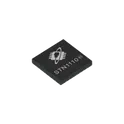
STN1110-IMM General Description The STN1110-IMM is a multiprotocol OBD-II to UART interpreter integrated circuit designed for automotive diagnostic, telematics, and vehicle communication applications. The device translates OBD-II network traffic into a UART serial data stream for communication with external microcontrollers, embedded processors, and host systems. It supports all legislated OBD-II protocols and provides compatibility with ELM327-based software while offering enhanced processing performance, expanded memory resources, advanced message filtering, firmware upgrade capability, and low-power operation. The device is intended for use in automotive diagnostic tools, fleet management systems, vehicle monitoring equipment, data acquisition systems, and embedded automotive communication products. Engineering Specification Part Number: STN1110-IMM Component Type: OBD-II to UART Interpreter Integrated Circuit Device Category: Automotive Communication Interface IC Package Type: QFN Mounting Type: Surface Mount Device (SMD) Interface Type: * UART * OBD-II Supported Protocols: * ISO 15765-4 CAN * ISO 14230-4 KWP2000 * ISO 9141-2 * SAE J1850 PWM * SAE J1850 VPW Key Features: * Multiprotocol OBD-II support * ELM327 command compatibility * Enhanced ST command extensions * High-speed UART communication * Advanced message filtering * Firmware upgrade capability * Large message buffering * Low-power operation * Automotive diagnostic interface functionality Applications: * OBD-II Scan Tools * Vehicle Diagnostics * Automotive Telematics * Fleet Management Systems * Data Logging Equipment * Embedded Automotive Controllers * Emissions Monitoring Systems * Vehicle Communication Gateways Tags #commonpartslibrary #integratedcircuit #ic #automotive #automotiveelectronics #automotivediagnostics #obdii #obd #uart #vehiclecommunication #telematics #embeddedsystems #communicationinterface #diagnosticinterface #scantool #canbus #kwp2000 #saej1850 #iso9141 #surfaceMount #smd #qfn #electroniccomponent #semiconductor #vehicleelectronics #microcontrollerinterface #datalogging #fleetmanagement #embeddedhardware #hardwaredesign
4 Uses0 Stars