Interface ICs
An interface IC is a type of integrated circuit that is designed to facilitate communication between two devices or systems. These devices are commonly used in electronic systems to enable the transfer of data and control signals between different components or subsystems. Some common use cases for interface ICs include connecting microcontrollers to peripherals such as sensors or displays, linking multiple processors together in a network, and enabling communication between devices using different communication protocols. Flux.ai has the world's largest community-driven public library of interface ICs, with footprints, symbols, datasheets, and simulation models. This library is a valuable resource for engineers and designers who need access to accurate and up-to-date information on these important components. Whether you are working on a new design project or simply looking to learn more about interface ICs, Flux.ai is an excellent resource to help you find the information you need.
MPU-6050
Accelerometer, Gyroscope, 6 Axis Sensor I²C Output 6-axis MEMS motion tracking sensor integrating a 3-axis gyroscope, 3-axis accelerometer, and digital temperature sensor. Operates from a 2.375 V to 3.46 V supply, communicates via an I²C interface (up to 400 kHz), and provides programmable gyroscope ranges of ±250, ±500, ±1000, and ±2000 °/s and accelerometer ranges of ±2 g, ±4 g, ±8 g, and ±16 g. Includes an on-chip Digital Motion Processor (DMP) and supports operation over a -40°C to +85°C temperature range. #TDKInvenSense #MPU6050 #IMU #MotionSensor #MEMS #Accelerometer #Gyroscope #I2C #DigitalMotionProcessor #EmbeddedSystems #commonpartslibrary #sensor #transducer #accelerometer
388 Uses0 StarsBSC030N10NS5SCATMA1
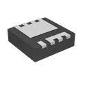
N-Channel 100 V 171A (Tc) 188W (Tc) Surface Mount PG-WSON-8-2 The BSC030N10NS5SCATMA1 specification defines the engineering requirements for an N-channel power MOSFET designed for high-efficiency switching and power management applications. This specification establishes the functional, electrical, mechanical, thermal, environmental, and quality requirements necessary to ensure reliable switching performance, low conduction losses, and long-term operational stability in power electronic systems. The device is intended for use in DC-DC converters, synchronous rectification circuits, motor control systems, battery management systems, power distribution modules, and industrial electronic equipment. It provides low on-state resistance, fast switching characteristics, and efficient power handling, making it suitable for high-frequency and high-current applications requiring optimized efficiency and thermal performance. Engineering Requirements The power MOSFET shall be manufactured using advanced semiconductor fabrication processes and qualified materials to ensure consistent electrical characteristics, high switching efficiency, and reliable long-term operation. The device shall maintain stable performance under specified voltage, current, and environmental operating conditions. Electrical characteristics shall provide low on-state resistance, high current-carrying capability, low gate charge, and fast switching performance to minimize conduction and switching losses. The device shall maintain stable operation during repetitive switching cycles, transient load conditions, and dynamic power management applications. Thermal performance shall support efficient heat dissipation through the package structure and printed circuit board interface. The component shall maintain electrical integrity and operational reliability within the specified junction temperature range during continuous and intermittent high-power operation. Mechanical construction shall be suitable for automated surface-mount assembly and compatible with standard solder reflow manufacturing processes. The package shall withstand vibration, thermal cycling, mechanical handling, and environmental exposure without degradation of electrical or mechanical performance. Workmanship shall be free from defects including contamination, cracks, bond failures, package deformation, or structural inconsistencies. Inspection, validation, and testing shall be conducted using calibrated equipment and controlled quality procedures to verify compliance with all applicable engineering and manufacturing requirements. Any deviation from this specification shall require formal engineering evaluation, documented technical justification, and approval through the established engineering change control process. Documentation Supporting documentation shall include engineering drawings, electrical performance specifications, thermal characterization reports, qualification records, inspection reports, material declarations, reliability data, and revision-controlled manufacturing documentation. All documentation shall be maintained under formal configuration management and quality assurance systems to ensure complete product traceability. Revision Control Any modification to this specification shall be managed through the formal engineering change management process. All revisions shall undergo technical review, validation, and approval before implementation to ensure continued compliance with design intent and applicable engineering standards. #EngineeringSpecification #PowerMOSFET #NChannelMOSFET #PowerElectronics #PowerManagement #MotorControl #DCDCConverter #Semiconductor #QualityAssurance #EngineeringDocumentation #commonpartslibrary #transistor #mosfet
0 Uses0 StarsPCM1822IRTER
ADC, Audio 32 b 8k ~ 192k I2S 20-WQFN (3x3) The PCM1822 is a high-performance, Burr-Brown™ audio analog-to-digital converter (ADC) that supports simultaneous sampling of up to two analog channels. The device supports single-ended and differential line and microphone inputs with a 1-VRMS full-scale signal. The device integrates a phase-locked loop (PLL), a DC removal high-pass filter (HPF), and supports sample rates up to 192 kHz. The device supports time-division multiplexing (TDM) or I2S audio formats, selectable with the hardware pin level. Additionally, the PCM1822 supports master and slave mode selection for the audio bus interface operation. These integrated high-performance features, along with the ability to be powered from a single supply of 3.3 V, make the device an excellent choice for costsensitive, space-constrained audio systems in far-field microphone recording applications. The PCM1822 is specified from –40°C to +125°C, and is offered in a 20-pin WQFN package. Features • Stereo high-performance ADC: – 2-channel analog microphones or line-in • ADC line and microphone differential and singleended input performance: – PCM1822 dynamic range: • 117-dB, dynamic range enhancer enabled • 111-dB, dynamic range enhancer disabled – THD+N: –95 dB • 1-VRMS full-scale input • ADC sample rate (fS) = 8 kHz to 192 kHz • Hardware pin control configurations • Linear-phase or low-latency filter selection • Flexible audio serial data interface: – Master or slave interface selection – 32-bits, 2-channel TDM – 32-bits, 2-channel I2S • Automatic power-down upon loss of audio clocks • Integrated high-performance audio PLL • Single-supply operation: 3.3 V • I/O-supply operation: 3.3 V or 1.8 V • Power consumption for 3.3-V AVDD supply: – 19.6 mW/channel at 16-kHz sample rate – 21.3 mW/channel at 48-kHz sample rate #CommonPartsLibrary #IntegratedCircuit #PCM1822IRTER #TexasInstruments #AudioADC #StereoADC #BurrBrown #I2S #TDM #AudioElectronics #EmbeddedAudio #SmartSpeaker #AVReceiver #HighResolutionAudio #PCBDesign #ElectronicsDesign #SignalProcessing
2 Uses0 StarsIS66WVH64M8DBLL-166B1LI
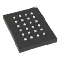
PSRAM (Pseudo SRAM) Memory IC 512Mbit HyperBus 166 MHz 36 ns 24-TFBGA (6x8) The IS66/67WVH64M8DALL/BLL are 512Mb Dual Die device containing two units of 256Mbit Pseudo Static Random Access Memory, organized as 64M words by 8 bits. The device supports a HyperBus interface, Very Low Signal Count (Address, Command and data through 8 DQ pins), Hidden Refresh Operation, and Automotive Temperature Operation, designed especially for Mobile and Automotive applications Key Features 512-Mbit (64M × 8) HyperRAM™ PSRAM High-speed HyperBus interface Clock frequency up to 166 MHz Fast 36 ns access time Single-ended clock architecture with reduced pin count Operating voltage range: 2.7 V to 3.6 V Industrial temperature range: −40°C to +85°C Low-power volatile memory solution Surface-mount 24-TFBGA (6 mm × 8 mm) package Suitable for graphics, AI edge devices, networking, and embedded systems requiring large external memory capacity. #CommonPartsLibrary #IntegratedCircuit #HyperRAM #PSRAM #ISSI #MemoryIC #HyperBus #EmbeddedSystems #IndustrialElectronics #IoT #HighSpeedMemory #BGA #VolatileMemory #EdgeComputing #HMI #ElectronicsDesign
2 Uses0 StarsDRV8770RGER
Half Bridge (2) Driver DC Motors, General Purpose NMOS, Power MOSFET 24-VQFN (4x4) The DRV8770RGER is a high-voltage brushed DC motor gate driver integrated circuit manufactured by Texas Instruments, designed to drive external N-channel power MOSFETs configured in a dual half-bridge topology for use in brushed DC motor control, stepper motor drive, solenoid actuation, and other inductive load switching applications. Rather than integrating the power stage transistors directly within the IC, the DRV8770 functions as a gate driver, providing the gate voltage and current needed to fully and rapidly switch external discrete power MOSFETs, which allows the designer to choose power devices appropriate to the specific voltage and current requirements of their motor or load without being constrained by the internal power stage of an integrated motor driver. The DRV8770 delivers two half-bridge gate drivers, each capable of driving high-side and low-side N-channel power MOSFETs. The integrated bootstrap diode and external capacitor generate the correct gate drive voltages for the high-side MOSFETs, while the GVDD rail drives the gates of the low-side MOSFETs. This bootstrap architecture eliminates the need for an external isolated gate drive power supply for the high-side switch, simplifying the overall power stage design significantly compared to approaches that require separate high-side power supply generation. This device decreases system component count, reduces PCB area, and saves cost by integrating two independent half-bridge gate drivers and bootstrap diodes. digikeyTME The high-side and low-side gate drivers can drive source and sink currents sufficient for fast, efficient switching of external power MOSFETs, with total average output current capability defined in the datasheet. The asymmetric source and sink current capability is a deliberate design choice reflecting the typical requirements of power MOSFET switching, where rapid turn-off is often more critical than turn-on speed for preventing shoot-through and managing switching losses in bridge circuits. Small propagation delay and delay matching specifications minimize the dead-time requirement, which further improves efficiency. TMEFarnell The high voltage tolerance of the gate drive pins improves system robustness. The SHx phase pins can tolerate significant negative voltage transients, while the high-side gate driver supply can support higher positive voltage transients on the BSTx and GHx pins. This enhanced transient tolerance is essential in motor drive applications where inductive switching generates voltage spikes and negative voltage excursions on the switch node that would damage less robust gate driver designs. An input deglitcher prevents high-frequency noise on the input pins from affecting the output state of the gate drivers, protecting against inadvertent switching caused by electrical noise on the control interface lines. FarnellAllDataSheet The device can drive one or two DC brush motors, one stepper motor, solenoids, or other inductive loads. This versatility makes it suitable across a broad range of actuator types within the same hardware platform, allowing a single PCB design to serve multiple product variants by simply changing the connected load and the firmware control scheme. Undervoltage protection is provided for both low-side and high-side through GVDD and BST undervoltage lockout, preventing the external power MOSFETs from operating with insufficient gate drive voltage, which would cause them to enter a linear operating region with excessive power dissipation and potential thermal damage. digikeyFarnell The DRV8770RGER is housed in a compact VQFN twenty-four-pin surface-mount package, suited to space-constrained motor drive PCB layouts, and is rated for operation across an extended industrial temperature range. Spec Sheet Identification Part Number: DRV8770RGER Device Family: DRV8770 Manufacturer: Texas Instruments Functional Classification Device Type: Dual half-bridge N-channel MOSFET gate driver IC Topology: Two independent half-bridge gate drivers Application Class: Brushed DC motor, stepper motor, solenoid, and inductive load drive Gate Drive Architecture High-Side Driver: Bootstrap-based gate drive with integrated bootstrap diode Low-Side Driver: GVDD-referenced direct gate drive Gate Drive Current — Source: High source current capability for rapid MOSFET turn-on Gate Drive Current — Sink: Higher sink current capability for rapid MOSFET turn-off Voltage Ratings Maximum Operating Voltage: High-voltage class, suited to industrial motor supply rails Phase Pin Transient Tolerance: Rated for negative voltage transients on SHx switch node pins Bootstrap Pin Transient Tolerance: Elevated absolute maximum on BSTx and GHx pins for spike immunity Timing & Switching Performance Propagation Delay: Small and tightly specified for minimal dead-time requirement Delay Matching: High-side to low-side delay matching for improved bridge efficiency Input Deglitching: Built-in input deglitch filter to suppress high-frequency noise on control inputs Protection Features GVDD Undervoltage Lockout: Protects low-side gate drive from insufficient supply BST Undervoltage Lockout: Protects high-side gate drive from insufficient bootstrap voltage Negative Transient Tolerance: Phase pins rated for switch-node negative voltage excursions Load Compatibility Supported Load Types: Brushed DC motors, stepper motors, solenoids, and general inductive loads Drive Configurations: Single or dual brushed DC motor, single stepper motor, or independent half-bridge loads Environmental & Qualification Operating Temperature Range: Extended industrial temperature range RoHS Compliance: Yes Lifecycle Status: Active production Package Package Type: VQFN — Very thin Quad Flat No-Lead, twenty-four-pin Package Suffix: RGER designation Mounting Method: Surface mount technology (SMT) Package Pitch: Fine pitch, compact footprint Packaging Format Supply Format: Tape-and-reel, cut-tape, and custom reel options available #DRV8770 #DRV8770RGER #TexasInstruments #GateDriver #HalfBridgeDriver #BrushedDCMotor #MotorDriver #StepperMotorDriver #SolenoidDriver #NChannelMOSFET #BootstrapDriver #HighVoltageDriver #PowerElectronics #MotorControl #InductiveLoad #VQFN #SurfaceMount #SemiconductorIC #EngineeringSpec #ComponentLibrary #CommonPartsLibrary #RoHSCompliant #IndustrialMotorDrive
2 Uses0 StarsIQS7222B102QNR
All details fully confirmed from Azoteq's official IQS7222B datasheet and multiple verified distributor sources. Here's the complete spec. Engineering Specification — IQS7222B102QNR Manufacturer: Azoteq (Pty) Ltd Device Family: IQ Switch® ProxFusion® Series — IQS7222B General Description The IQS7222B102QNR is a high-channel-count capacitive touch and proximity sensing controller integrated circuit manufactured by Azoteq, belonging to the ProxFusion series of intelligent human interface sensing devices. The IQS7222B is a sensor fusion device for various multi-button applications that is fully I²C compatible, with on-chip calculations that enable the IC to respond effectively even in the lowest-power modes. It represents an expanded-channel evolution within Azoteq's IQS7222 family, offering a substantially higher mutual capacitance channel count than the IQS7222A variant while maintaining the same ProxFusion design philosophy of combining sophisticated on-chip sensing intelligence with a minimal external component requirement and a compact surface-mount package. Molex The IQS7222B is a highly flexible ProxFusion device that can configure up to eighteen mutual capacitance buttons or up to eight self-capacitance buttons, with nine external sensor pad connections available in the QFN package variant. Alternatively, it can configure up to twenty mutual capacitance buttons or eighteen mutual capacitance buttons with a proximity wake-up function. This high degree of channel configurability makes the device adaptable to a very broad range of physical interface configurations, from simple multi-button panels to complex touch arrays with simultaneous proximity wake-up capability, all within a single fixed-footprint IC that does not require a change of device between product variants with different button counts. MolexAmazon Target applications for the IQS7222B include remote control user interfaces, home automation device user interfaces, and wireless speaker controls. These application domains share common requirements for robust touch detection through cosmetic overlay materials such as glass, plastic, or painted surfaces, reliable operation in environments where the device may be exposed to moisture or contamination, and power efficiency sufficient to support battery-powered or always-on operation without significantly impacting battery life. The device's on-chip power management architecture, which features automated system power modes for optimal response versus consumption, directly addresses these requirements by allowing the device to spend the majority of its time in a low-current sleep or ultra-low-power state while still waking promptly in response to proximity or touch events. MolexMolex Built-in basic functions include automatic tuning, noise filtering, debounce and hysteresis, and dual direction trigger indication. The automatic tuning capability, implemented through Azoteq's proprietary ATI algorithm, compensates for variations in electrode capacitance that arise from PCB manufacturing tolerances, overlay thickness variation, and environmental factors such as temperature and supply voltage drift. This self-calibration eliminates the need for individual unit factory calibration and ensures consistent touch sensitivity across the full production run of any product built around this device. The noise filtering and debounce functions further improve the reliability of touch event detection in electrically noisy environments, preventing false triggers from electrical interference or mechanical vibration that could otherwise cause spurious button events in poorly filtered designs. Molex Both mutual capacitance and self-capacitance designs are possible with the IQS7222B, giving system designers the flexibility to choose the sensing modality most appropriate for their electrode layout and overlay configuration. Mutual capacitance sensing offers better noise immunity and the ability to detect touch through thicker overlay materials, while self-capacitance sensing allows a simpler single-electrode layout per button with potentially higher raw sensitivity. The I²C communication interface supports IRQ/RDY signaling at speeds up to Fast-Plus mode, providing efficient, low-latency event notification to the host microcontroller without requiring continuous polling of the device. The "QNR" suffix in the part number designates the QFN twenty-pin package variant, which offers the maximum external pad count for mutual capacitance configurations. MolexMolex Spec Sheet Identification Part Number: IQS7222B102QNR Device Family: IQ Switch ProxFusion Series — IQS7222B Manufacturer: Azoteq (Pty) Ltd Part Number Decode IQS7222B: Base device family, B-variant expanded channel count 102: Firmware/configuration variant designation QNR: QFN twenty-pin package, tape-and-reel Functional Classification Device Type: Multi-channel capacitive touch and proximity sensing controller IC Sensing Architecture: ProxFusion sensor fusion engine with on-chip processing Application Class: Multi-button, slider, and wheel human interface controller Channel Configuration Mutual Capacitance Buttons: Up to twenty configurable buttons Mutual Capacitance with Proximity Wake-Up: Up to eighteen mutual capacitance buttons with simultaneous proximity wake function Self-Capacitance Buttons: Up to eight self-capacitance buttons External Sensor Pad Connections: Nine pads available in QFN package Sensing Modalities Mutual Capacitance: Full channel array for high noise immunity and overlay penetration Self-Capacitance: Simplified single-electrode per button layout option Proximity Detection: Pre-touch proximity wake-up capability Built-In Processing Functions Automatic Tuning: Proprietary ATI algorithm for self-calibration and baseline normalization Noise Filtering: Integrated digital filtering for EMI and environmental noise rejection Debounce and Hysteresis: Per-channel configurable debounce and release hysteresis Dual Direction Trigger: Positive and negative delta event detection Host Interface Communication Protocol: I²C fully compatible Speed Grade: Up to Fast-Plus mode Event Signaling: IRQ/RDY interrupt output for host notification I²C Address: Configurable; additional address options available on special request Power Management Operating Modes: Active sensing, idle, and ultra-low-power modes Automated Power Mode Control: System-managed transitions for optimized response versus current consumption ULP Wake Capability: Proximity or touch event wake-up from ultra-low-power state Layout & Application Notes VREG Decoupling: Capacitor required at each VREG pin, placed as close as possible to IC Tx Series Resistance: Nominal series resistance recommended on Rx electrodes to reduce EMI coupling ESD Rating: Pins rated to high HBM ESD performance per JEDEC JEP155 Environmental & Qualification RoHS Compliance: Yes Lifecycle Status: Active production Package Package Type: QFN — Quad Flat No-Lead, twenty-pin Package Designation: QNR variant per Azoteq ordering suffix Mounting Method: Surface mount technology (SMT) Packaging Format Supply Format: Tape-and-reel Target Applications Remote control user interfaces Home automation device controls Wireless speaker and audio device interfaces Multi-button consumer appliance panels IoT device touch interfaces Industrial HMI panels with overlay #IQS7222B #IQS7222B102QNR #Azoteq #ProxFusion #IQSwitch #CapacitiveTouchController #MutualCapacitance #SelfCapacitance #ProximityController #MultiButtonHMI #TouchSensor #ATICalibration #SmartHMI #HomeAutomation #RemoteControl #WirelessSpeaker #IoTDesign #LowPowerSensing #QFN20 #SurfaceMount #EmbeddedHMI #EngineeringSpec #ComponentLibrary #CommonPartsLibrary #RoHSCompliant
2 Uses0 StarsIQS7222A001CSR
Capacitive Touch Buttons, Slider, Wheel 18-WLCSP (1.62x1.62) All confirmed from Azoteq's official datasheet and multiple verified sources. Here's the complete spec. Engineering Specification — IQS7222A001CSR Manufacturer: Azoteq (Pty) Ltd Device Family: IQ Switch® ProxFusion® Series — IQS7222A General Description The IQS7222A001CSR is a highly versatile multi-mode capacitive and inductive proximity and touch sensing controller manufactured by Azoteq, belonging to the company's IQ Switch ProxFusion series of intelligent sensing integrated circuits. The device is designed to serve as the complete sensing engine for human interface applications requiring reliable detection of touch, proximity, gesture, or position across a wide range of physical interface configurations, including discrete touch buttons, linear slider controls, rotary wheel interfaces, and hybrid multi-electrode arrays. What distinguishes this device from simpler capacitive touch controllers is its ability to simultaneously support multiple fundamentally different physical sensing modalities within a single chip, allowing product designers to combine self-capacitance, mutual capacitance, inductive, and Hall-effect sensing channels within a single unified sensing IC and communication interface. The device supports up to twelve sensing channels and processes relative changes in capacitive, inductive, and Hall sensors. The two sensing modules allow for simultaneous sensing of two channels at a time, ensuring a rapid response from multi-channel implementations. Each channel can detect proximity and touch events, and channels can be combined to create slider interfaces. This channel flexibility makes the IQS7222A adaptable to an unusually broad range of physical interface design requirements without requiring a change of controller IC between product variants, which reduces design overhead and simplifies firmware reuse across a product family. Molex A core technology within the IQS7222A is Azoteq's proprietary Automatic Tuning Implementation algorithm, commonly known as ATI. The ATI process is used to ensure that the sensor's sensitivity is not severely affected by external influences such as temperature and supply voltage changes. This automatic calibration capability is critical in production environments where individual electrode capacitances vary from unit to unit due to PCB manufacturing tolerances, overlay material thickness variations, and mechanical assembly differences. Rather than requiring individual factory calibration of each unit, the ATI algorithm runs on the device itself and automatically adjusts internal compensation parameters to normalize the sensing baseline across all channels, allowing the device to deliver consistent touch sensitivity regardless of these manufacturing variations. Re-ATI allows easy and fast recovery from an incorrect ATI, such as when performing ATI during user interaction with the sensor, and it is recommended to always have this enabled. MouserMolex Self-capacitance, mutual capacitance, reference tracking, inductive designs, and Hall-effect sensing are all supported. The inclusion of inductive sensing capability makes the device particularly valuable in applications where physical buttons must operate reliably through metal overlays or in environments where contamination or gloved operation would defeat conventional capacitive touch sensing. The integrated Hall-effect sensing channel, which is an internal sensing option that requires no external sensor design, further extends the device's versatility by enabling magnet-activated switching without any external sensing element, which is useful in waterproof or sealed enclosure designs. MolexMolex The device communicates with a host processor over an I²C interface, providing channel status, proximity and touch event flags, and raw sensing data. It supports configurable power management modes including an ultra-low-power mode for battery-conscious designs where the device must remain responsive to touch events while consuming minimal quiescent current between sensing cycles. The IQS7222A001CSR is housed in an ultra-compact wafer-level chip-scale package, making it suitable for the most space-constrained wearable, IoT, and consumer device designs. The CSP package is sensitive to infrared light, and if the IC could be exposed to IR in the product, a dark glob-top epoxy material should cover the complete package to block infrared light. Molex Spec Sheet Identification Part Number: IQS7222A001CSR Device Family: IQ Switch ProxFusion Series — IQS7222A Manufacturer: Azoteq (Pty) Ltd Functional Classification Device Type: Multi-mode capacitive, inductive, and Hall-effect proximity and touch sensing controller IC Sensing Architecture: Dual-module simultaneous sensing engine Channel Count: Up to twelve sensing channels Supported Sensing Modalities Self-Capacitance Sensing: Up to full channel count in self-capacitance configuration Mutual Capacitance Sensing (Projective): Supported for improved noise immunity and hover detection Self-Capacitance with Wear Detection: Supported channel variant Inductive Sensing: Supported for metal overlay and through-metal applications Hall-Effect Sensing: Integrated internal Hall channel, no external sensor required Interface Types Supported Discrete Touch Buttons: Multi-channel button arrays Linear Slider: Multi-electrode slider position sensing Rotary Wheel: Circular gesture and angular position sensing Proximity Detection: Pre-touch proximity event reporting Automatic Tuning ATI Technology: Proprietary Automatic Tuning Implementation for self-calibration Re-ATI: Automatic re-calibration recovery, recommended always enabled Baseline Tracking: Long-term average tracking with configurable halt behavior Host Interface Communication Protocol: I²C interface Event Reporting: Per-channel proximity and touch event flags Raw Data Access: Sixteen-bit count values per channel Power Management Ultra-Low-Power Mode: Configurable ULP entry with touch-wake capability Operating Modes: Active, idle, and ultra-low-power configurable states Protection & Layout Notes IR Sensitivity: CSP package sensitive to infrared light — dark glob-top epoxy recommended if IR exposure possible Decoupling: VDD and VREG decoupling capacitors must be placed as close as possible to respective pads Environmental & Qualification RoHS Compliance: Yes Lifecycle Status: New product, active production Package Package Type: WLCSP — Wafer-Level Chip Scale Package Pin Count: Eighteen ball WLCSP Mounting Method: Surface mount technology (SMT) Packaging Format Supply Format: Tape-and-reel #IQS7222A #Azoteq #ProxFusion #IQSwitch #CapacitiveTouchController #TouchSensor #ProximitySensor #MultiModeSensor #InductiveSensing #HallEffectSensor #SelfCapacitance #MutualCapacitance #ATICalibration #SliderControl #TouchButton #RotaryWheel #WLCSP #UltraCompact #WearableElectronics #IoTDesign #HMIDesign #EmbeddedSystems #EngineeringSpec #ComponentLibrary #CommonPartsLibrary #RoHSCompliant
0 Uses0 StarsBC847
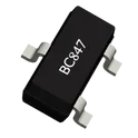
All details fully confirmed across multiple authoritative sources including Nexperia, ROHM, Farnell, and others. Here's the complete spec. Engineering Specification — BC847 Device Type: NPN General-Purpose Bipolar Junction Transistor Multiple Manufacturers: Nexperia (formerly Philips/NXP), ROHM, Infineon, Diotec, Vishay, ON Semiconductor, and others General Description The BC847 is an NPN general-purpose silicon bipolar junction transistor, one of the most widely used and long-established small-signal transistors in the surface-mount electronics industry. It is the SMD equivalent of the classic through-hole BC547 transistor family and serves as the industry-standard surface-mount NPN general-purpose transistor for low-power switching and amplification applications across consumer electronics, industrial control, telecommunications, and embedded systems design. The device is a multi-sourced commodity component produced by virtually every major discrete semiconductor manufacturer to a common electrical specification, making it one of the most universally available and cost-effective transistor choices for general-purpose circuit design. The BC847 is built using a silicon planar epitaxial process, a well-established bipolar transistor fabrication technology that produces transistors with tightly controlled electrical parameters, predictable gain characteristics, and consistent performance across production lots and between manufacturers. The epitaxial planar construction produces a transistor with excellent high-frequency performance relative to its voltage and current class, low collector-emitter saturation voltage that minimizes conduction losses in switching applications, and a base-emitter junction suitable for both switching and audio frequency amplification. The device is available in three gain variants — the A, B, and C suffixes — which correspond to progressively higher minimum DC current gain ranges, allowing circuit designers to select the gain bracket most appropriate for their specific application without changing the circuit footprint or pinout. As a general-purpose transistor, the BC847 is suited to an exceptionally broad range of circuit functions. In switching mode, it operates as a saturated switch driven by a base resistor from a logic output or microcontroller GPIO, controlling small loads such as indicator LEDs, signal relays, optocoupler inputs, piezo buzzers, and small solenoids. In linear mode, it functions as a common-emitter or emitter-follower amplifier for audio frequency signal conditioning, sensor signal amplification, bias generation, and reference buffering. Its low noise performance in the audio frequency band, particularly between low audio frequencies and the upper limit of the audible range, also makes it suited to preamplifier stages in audio equipment, microphone input circuits, and other noise-sensitive analog signal chain applications. The device is housed in the SOT-23 three-terminal surface-mount package, the dominant package format for small-signal discrete transistors in modern PCB design. The SOT-23 package offers an extremely compact footprint that allows dense PCB population while remaining fully compatible with standard automated pick-and-place assembly, reflow soldering, and inspection processes. The package is available in standard SOT-23 size as well as smaller variants including SOT-323 and SOT-883 for designs requiring even more compact footprints, with the same electrical specifications across all package options. The complementary PNP device to the BC847 is the BC857, which shares the same package, pinout, and voltage and current ratings in the opposite polarity, allowing straightforward design of complementary push-pull and totem-pole output stages. Spec Sheet Identification Part Number: BC847 (suffixes A, B, C denote gain groups) Device Family: BC847 series, NPN general-purpose transistor Manufacturer: Multi-sourced commodity part — Nexperia, ROHM, Infineon, Diotec, Vishay, ON Semiconductor, and others PNP Complement: BC857 Functional Classification Device Type: NPN bipolar junction transistor (BJT) Construction: Silicon planar epitaxial Application Class: General-purpose switching and amplification Gain Variants BC847A: Lowest gain range group BC847B: Mid gain range group BC847C: Highest gain range group Absolute Maximum Ratings Collector-Emitter Voltage: Standard low-voltage small-signal transistor class Collector-Base Voltage: Slightly higher than collector-emitter rating Emitter-Base Voltage: Standard emitter-base reverse voltage class Collector Current: Low continuous current class, suitable for signal and small load switching Peak Collector Current: Higher pulsed current capability Total Power Dissipation: Low power dissipation class, standard for SOT-23 package Operating Junction Temperature: Extended range, standard silicon transistor class Electrical Characteristics DC Current Gain: Variant-dependent, high gain class for general-purpose applications Collector-Emitter Saturation Voltage: Low saturation voltage for efficient switching Base-Emitter Saturation Voltage: Standard silicon junction voltage class Collector Cutoff Current: Low leakage class Transition Frequency: High-frequency capable for audio and signal switching applications Noise Figure: Low noise in audio frequency band Package & Mechanical Primary Package: SOT-23 (TO-236AB) Alternate Packages: SOT-323 (SC-70), SOT-883 (DFN1006-3) — same electrical specs Mounting Method: Surface mount technology (SMT) Pin Configuration: Base — Pin 1, Emitter — Pin 2, Collector — Pin 3 Target Applications Logic-level switching of LEDs, relays, and small loads Audio frequency signal amplification and preamplification Sensor signal conditioning and buffering Emitter follower and bias circuits Optocoupler and interface drive circuits General-purpose analog and digital circuit design Environmental & Qualification RoHS Compliance: Yes, lead-free across all manufacturer sources Flammability Rating: UL94 V-0 package material Packaging Supply Format: Tape-and-reel, per manufacturer standard packaging #BC847 #BC847B #BC847C #NPNTransistor #BipolarTransistor #BJT #SmallSignalTransistor #GeneralPurposeTransistor #SOT23 #SurfaceMountTransistor #SwitchingTransistor #AmplifierTransistor #LowPowerTransistor #SiliconEpitaxial #BC857Complement #DiscreteComponent #AnalogCircuit #EmbeddedSystems #EngineeringSpec #ComponentLibrary #CommonPartsLibrary #RoHSCompliant #CommodityPart
14 Uses0 StarsSSQ-110-03-T-D
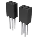
20 Position Receptacle Connector 0.100" (2.54mm) Through Hole Tin The SSQ-110-03-T-D is a through-hole dual-row socket strip receptacle connector manufactured by Samtec, designed for board-to-board and pin header mating applications using the industry-standard pitch spacing that has been dominant in through-hole PCB interconnect design for decades. It belongs to Samtec's SSQ series, a family of square-post socket strip connectors that accept standard square-pin headers and are widely used across prototyping, instrumentation, test and measurement, embedded systems, industrial control, and general-purpose PCB stacking applications. As a socket strip of the receptacle gender, the SSQ-110-03-T-D is intended to receive a mating male pin header, creating a reliable and separable board-to-board or wire-to-board connection. The dual-row configuration provides a higher contact density within a given board length than a single-row socket, which is why dual-row socket strips in this pitch class are extensively used in applications such as microcontroller and single-board computer expansion connectors, module-to-baseboard interfaces, and other designs where a significant number of signal, power, or ground connections must be made across a single separable connector interface. The connector features square solder tails for through-hole PCB mounting, with the "-T" suffix in the part number designating the square post tail style, which provides a well-defined mechanical footprint and reliable solder joint formation in wave solder and hand-solder assembly processes. The "-D" suffix indicates the dual-row configuration. Contact material is phosphor bronze, a widely used spring-contact alloy chosen for its combination of good electrical conductivity, excellent spring properties that maintain consistent contact force across many mating cycles, and resistance to stress relaxation over time. The contacts are finished with matte tin plating over nickel underplate, providing a solderable, cost-effective contact surface suitable for the majority of general-purpose signal and low-power applications for which this connector class is typically used. The insulator body is molded from black liquid crystal polymer, a high-performance engineering thermoplastic that offers the high dimensional stability, excellent electrical insulation properties, and high-temperature resistance needed to withstand wave soldering and reflow-adjacent thermal exposure during PCB assembly. The material also carries a UL94 V-0 flammability rating, reflecting its self-extinguishing behavior in the event of an ignition source, which is required or preferred in many end-product regulatory compliance frameworks. The SSQ series is widely used in conjunction with Samtec's TSW series male pin headers as a complementary mating pair, and the connector is compatible with a broad range of standard square-pin headers from other manufacturers that conform to the same pitch and pin geometry, making it a versatile choice for general-purpose through-hole header applications. Spec Sheet Identification Part Number: SSQ-110-03-T-D Series: SSQ Manufacturer: Samtec, Inc. Connector Type / Configuration Type: Socket strip receptacle Gender: Female (receptacle) Row Configuration: Dual row Orientation: Straight, vertical Mounting Method: Through-hole, solder tail Contact & Material Properties Contact Material: Phosphor bronze Contact Finish — Mating Zone: Matte tin over nickel Contact Finish — Post/Tail: Tin Contact Type: Forked socket, square post acceptance Post/Tail Style: Square solder tail Mechanical Specifications Contact Pitch: Standard pitch class, widely used through-hole spacing Profile Height: Standard SSQ series mated height class Insulator Color: Black Insulator Material: Liquid crystal polymer (LCP) Flammability Rating: UL94 V-0 Body Orientation: Straight Electrical Ratings Current Rating Per Contact: Mid-range per-pin current class Voltage Rating: High AC and DC voltage rating class for general-purpose signal use Mating Cycles: Rated for repeated mate/unmate cycles Environmental & Qualification Operating Temperature Range: Extended range, suitable for industrial environments RoHS Compliance: Yes Export Classification: EAR99 Mating Compatibility Mates With: Samtec TSW series male pin headers and compatible standard square-pin headers from other manufacturers Application Note: Suitable for board-to-board stacking, module-to-baseboard interfaces, SBC expansion connectors, and general-purpose through-hole header applications Packaging Supply Format: Bulk packaging #SSQ110 #Samtec #SocketStrip #DualRowConnector #ThroughHoleConnector #PCBReceptacle #PinHeader #BoardToBoard #FemaleSockets #PhosphorBronze #LCP #UL94V0 #EmbeddedSystems #Prototyping #InstrumentationConnector #GeneralPurposeConnector #ConnectorDatasheet #EngineeringSpec #ComponentLibrary #CommonPartsLibrary #RoHSCompliant #PCBDesign #CommonPartsLibrary #Connector #Header #Receptacle #Female-Socket #SSQ
38 Uses0 StarsIXTL2N470
N-Channel 4700 V 2A (Tc) 220W (Tc) Through Hole ISOPLUSi5-Pak™ Full picture confirmed from IXYS/Littelfuse datasheet sources — N-channel MOSFET, unipolar, ultra-high voltage class, housed in the ISOPLUS i5-Pak package. Here's the complete spec. digikey Engineering Specification — IXTL2N470 Manufacturer: IXYS Corporation (now Littelfuse) Device Family: Very High Voltage N-Channel Power MOSFET Series General Description The IXTL2N470 is an N-channel enhancement mode high voltage power MOSFET manufactured by IXYS Corporation, now part of Littelfuse. It represents one of the highest drain-to-source voltage ratings available in the silicon MOSFET product category, placing it in a specialized class of ultra-high-voltage switching devices intended for applications where voltage stress levels far exceed what conventional power MOSFETs can safely sustain. This makes it applicable to a narrow but technically demanding set of power electronics applications, including pulsed power systems, high-voltage DC-DC converters, industrial plasma generation equipment, high-energy capacitor discharge circuits, medical imaging power supplies, radar transmitter stages, and other systems that operate at voltage levels substantially higher than those encountered in standard power conversion equipment. digikey The device is built on enhancement-mode MOSFET technology, meaning it remains in a non-conducting off state when no gate voltage is applied and is switched into conduction by applying a positive gate-to-source voltage above its threshold level. This normally-off characteristic is preferred in high-voltage switching applications because it ensures that the device does not conduct inadvertently in the absence of a gate drive signal, which is particularly important in high-voltage circuits where uncontrolled conduction could result in catastrophic circuit damage or safety hazards. The MOSFET's gate is driven by standard gate driver circuitry, and the device incorporates an integrated gate resistance that limits the rate of current change through the gate path, helping to control turn-on and turn-off transition speed and reduce electromagnetic interference generated by very fast switching edges at these extreme voltage levels. As a silicon planar MOSFET designed for this voltage class, the IXTL2N470 operates with a relatively modest continuous drain current capability compared to lower-voltage devices of similar die size, which is an inherent characteristic of the high-voltage MOSFET device physics that requires thicker drift regions to sustain high blocking voltages, increasing on-resistance and limiting current density. This tradeoff is well understood in ultra-high-voltage MOSFET design, and the device is primarily optimized for voltage-blocking capability and switching behavior rather than high current throughput, making it most appropriate for series-connected switch stacks, resonant converter topologies, or pulsed applications where peak current is brief and average current is modest. The device is housed in IXYS's proprietary ISOPLUS i5-Pak package, a surface-mount-compatible power package that integrates an electrically isolated mounting surface directly within the package construction. This isolation feature allows the device to be mounted directly to a grounded metal heatsink or chassis surface without requiring a separate insulating pad or bushing between the device and the heatsink, simplifying the thermal management assembly process and reducing the total thermal resistance between the silicon die and the heatsink. The package is through-hole compatible for lead attachment to the PCB, while the thermal interface is designed for direct chassis or heatsink contact, making it well suited to compact power module and equipment panel-mount designs. Spec Sheet Identification Part Number: IXTL2N470 Device Family: Very High Voltage N-Channel Standard Power MOSFET Manufacturer: IXYS Corporation (now Littelfuse) Functional Classification Device Type: Power MOSFET Channel Type: N-channel Operating Mode: Enhancement mode (normally off) Technology: Silicon planar high-voltage MOSFET Electrical Characteristics Drain-to-Source Voltage Rating: Ultra-high voltage class, among the highest available in silicon MOSFET technology Drain Current Rating: Low continuous current class, consistent with ultra-high-voltage MOSFET physics Power Dissipation: High power dissipation class for its current rating, reflecting package thermal capability On-Resistance: Relatively high on-resistance, inherent to ultra-high-voltage MOSFET drift region design Gate Threshold: Standard enhancement-mode positive gate threshold voltage Integrated Gate Resistance: Built-in gate resistance for switching transition control and EMI reduction Input Capacitance: Moderate-to-high input capacitance class Reverse Transfer Capacitance: Low reverse transfer capacitance class Switching Characteristics Turn-On Delay: Defined turn-on delay time Rise Time: Defined output voltage rise time Turn-Off Delay: Defined turn-off delay time Fall Time: Defined output voltage fall time Thermal Characteristics Junction-to-Case Thermal Resistance: Defined by package construction and isolated mounting interface Operating Junction Temperature: Standard high-temperature silicon MOSFET class Mechanical & Package Package Type: ISOPLUS i5-Pak (proprietary IXYS isolated surface-mount power package) Isolation Feature: Electrically isolated mounting base integrated within package — no external insulator required for heatsink mounting Mounting Method: Through-hole PCB pin termination with isolated bottom thermal contact Environmental & Qualification RoHS Compliance: Yes Lifecycle Status: Active, available through Littelfuse and authorized distributors Target Applications Application Domains: Pulsed power systems, high-voltage DC-DC converters, plasma generation equipment, medical imaging power supplies, radar transmitter stages, capacitor discharge circuits, high-voltage series switch stacks #IXTL2N470 #IXYS #Littelfuse #HighVoltageMOSFET #UltraHighVoltageMOSFET #NChannelMOSFET #PowerMOSFET #EnhancementMode #ISOPLUSi5Pak #PulsedPower #HighVoltagePower #PowerElectronics #SwitchingDevice #PlasmaEquipment #MedicalPowerSupply #IndustrialPower #SemiconductorIC #DiscreteSemiconductor #EngineeringSpec #ComponentLibrary #CommonPartsLibrary #RoHSCompliant
1 Uses0 Stars