Interface ICs
An interface IC is a type of integrated circuit that is designed to facilitate communication between two devices or systems. These devices are commonly used in electronic systems to enable the transfer of data and control signals between different components or subsystems. Some common use cases for interface ICs include connecting microcontrollers to peripherals such as sensors or displays, linking multiple processors together in a network, and enabling communication between devices using different communication protocols. Flux.ai has the world's largest community-driven public library of interface ICs, with footprints, symbols, datasheets, and simulation models. This library is a valuable resource for engineers and designers who need access to accurate and up-to-date information on these important components. Whether you are working on a new design project or simply looking to learn more about interface ICs, Flux.ai is an excellent resource to help you find the information you need.
MMR920C04ARE
Pressure Sensor -0.57PSI ~ 0.57PSI (-3.92kPa ~ 3.92kPa) Gauge Male - 0.1" (2.5mm) Tube 7 b 12-SMD, No Lead, Top Port The MMR920C04ARE, manufactured by Mitsumi Electric, is a surface-mount pressure sensor that measures low differential (gauge) pressure with high accuracy. It integrates sensing, signal conditioning, and digital output in a single package, making it easy to interface with microcontrollers. Sensor Type: MEMS-based gauge pressure sensor Pressure Range: ±0.57 PSI (±3.92 kPa) Output Interface: Digital (supports I²C and SPI) Resolution: 7-bit output (internally higher-resolution processing available) Supply Voltage: 3.0 V to 3.6 V Accuracy: حوالي ±0.65% full scale Package: 12-SMD, no-lead, top-port (compact ~7×7×7.2 mm) Port Type: 2.5 mm tube (barbless) for airflow or gas connection Features: Built-in temperature compensation Fast sampling capability Factory-calibrated digital output #CommonPartsLibrary #Sensor #Pressure-Sensor #Transducer
0 Uses0 StarsAFE881H1RRUR
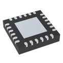
2 Channel AFE 16 Bit 24-UQFN (4x4) The AFE881H1RRUR is a highly integrated analog front-end (AFE) designed for multi-channel data acquisition systems. It combines precision analog signal conditioning with high-speed analog-to-digital conversion, making it suitable for applications such as medical instrumentation, industrial measurement, and test and measurement equipment. The device integrates low-noise amplifiers, programmable gain stages, anti-aliasing filters, and high-resolution ADCs into a compact package, reducing system complexity and board space. Key Features Multi-channel analog front-end integration High-resolution analog-to-digital conversion Low-noise input stage for precision measurements Programmable gain amplifier (PGA) Integrated anti-aliasing filters High sampling rate capability Serial digital interface (SPI-compatible) Low power consumption for portable systems Compact surface-mount package Electrical Characteristics (Typical – refer to datasheet for exact values) Supply Voltage: ~1.8 V to 3.3 V (analog/digital domains) Input Voltage Range: Dependent on configuration Resolution: Up to 16-bit or higher (device dependent) Sampling Rate: Up to several MSPS (depending on mode) Power Consumption: Optimized for performance/power balance Functional Blocks Low-noise input buffer Programmable gain amplifier (PGA) Anti-aliasing filter High-speed ADC core Digital control interface (SPI) Clock management circuitry Package Information Package Type: QFN / VQFN (exact variant per TI RRU package code) Mounting Type: Surface Mount Pin Count: Typically 40+ pins (refer to datasheet for exact count) Applications Medical imaging and instrumentation Industrial data acquisition systems Oscilloscopes and test equipment Communication systems Precision sensor interfaces Advantages High integration reduces external components Improved signal integrity due to low-noise design Flexible configuration via programmable gain Compact footprint for dense PCB layouts Notes Exact electrical parameters, pin configuration, and performance metrics must be verified in the official Texas Instruments datasheet. Proper PCB layout (grounding, shielding, and decoupling) is critical for optimal performance. #commonpartslibrary #integratedcircuit
1 Uses0 StarsSIM7600E-H
Cellular EDGE, GPRS, GSM, HSPA+, LTE, UMTS Transceiver Module 900MHz, 1.8GHz Antenna Not Included Surface Mount The SIM7600E-H is a multi-mode LTE module that supports: LTE (4G) Cat-4 with up to 150 Mbps download / 50 Mbps upload 3G (UMTS/HSPA+) 2G (GSM/GPRS/EDGE) fallback for global network compatibility It is built in a compact SMT/LCC package (about 30 × 30 mm) and is widely used for embedded devices that need mobile internet and GNSS positioning Key Features Network support LTE-FDD / LTE-TDD (global bands depending on variant) UMTS/HSPA+ GSM/GPRS/EDGE fallback Data speed LTE Cat-4: up to 150 Mbps downlink 3G/2G fallback for lower-speed connectivity GNSS built-in GPS / GLONASS / other satellite positioning support Interfaces USB 2.0 UART GPIO I2C ADC PCM (audio support) SIM card interface Software / protocols AT command control TCP/IP, UDP, HTTP, HTTPS, FTP, DNS Driver support for Windows, Linux, Android Power supply ~3.4V to 4.2V typical operating range Operating temperature -40°C to +85°C (industrial grade) Typical Applications IoT devices GPS trackers Smart metering Industrial routers / gateways Remote monitoring systems Vehicle telematics Point-of-sale terminals #commonpartslibrary #rf #wireless #transceiver #module
224 Uses0 StarsPEC06SAAN
Connector Header Through Hole 6 position 0.100" (2.54mm) The PEC06SAAN is a compact, low-cost incremental rotary encoder manufactured by Bourns. It is designed for user interface applications requiring precise rotational input, such as volume controls, menu navigation, and position sensing. This encoder provides reliable quadrature output signals and is suitable for through-hole PCB mounting. Its robust mechanical design ensures long operational life and consistent performance in consumer and industrial electronics. Key Features Incremental (relative) rotary encoder Compact, space-saving design Through-hole mounting configuration Quadrature output (A and B channels) Optional integrated push switch (depending on variant) Detent and non-detent options available High reliability with long rotational life RoHS compliant Electrical Characteristics Supply voltage: Typically 5 VDC (logic-level output) Output type: Digital quadrature (A/B signals) Contact resistance: ≤ 100 mΩ Insulation resistance: ≥ 100 MΩ @ 250 VDC Dielectric strength: 300 VAC for 1 minute Mechanical Characteristics Rotation type: Incremental Number of pulses per revolution (PPR): Typically 6 to 24 (variant dependent) Detent positions: Variant dependent Rotational torque: 10 to 70 gf·cm (typical range) Shaft length: Varies by suffix (e.g., 15 mm typical) Shaft type: Knurled or D-cut (variant dependent) Mounting type: Through-hole PCB Terminal type: PC pins Environmental Specifications Operating temperature range: −30°C to +70°C Storage temperature range: −40°C to +85°C Humidity: Up to 85% RH (non-condensing) Mechanical Life Rotational life: Up to 30,000 cycles (typical) Physical Dimensions Body size: Approximately 12 mm × 11 mm × 5 mm (excluding shaft) Shaft diameter: Typically 6 mm Pin pitch: Standard 2.54 mm Applications Consumer electronics (audio controls, appliances) Industrial control panels Embedded systems and microcontroller interfaces Automotive user interfaces Instrumentation and test equipment #commonpartslibrary #connector #header
32 Uses0 StarsSDP31-500Pa
Pressure Sensor -0.07PSI ~ 0.07PSI (-0.5kPa ~ 0.5kPa) Differential Male - 0.08" (2.00mm) Tube, Dual 16b 16-SMD Module, Dual Top Ports The SDP31-500PA belongs to the SDP3x series and uses Sensirion’s CMOSens® technology to deliver accurate and stable pressure measurements. It is optimized for applications where small size, fast response, and high accuracy are critical. This sensor measures bidirectional differential pressure up to ±500 Pa, making it suitable for airflow and gas flow monitoring systems. It provides a fully calibrated, temperature-compensated digital output via I²C, simplifying integration with microcontrollers. Pressure type: Differential (±500 Pa range) High accuracy: حوالي ±3% of measured value Digital output: I²C interface with 16-bit resolution Fast response time: suitable for real-time measurements No zero-point drift: ensures long-term stability Compact size: ~8.5 × 5.5 × 5.15 mm Low voltage operation: typically 3.0–3.6 V Temperature compensated: reliable from −40°C to +85°C #CommonPartsLibrary #Sensor #SDP3x
19 Uses0 StarsTDA4VM88TGCALFR
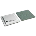
System On Chip (SOC) IC It integrates multiple processing units including CPUs, DSPs, AI accelerators, and GPU into a single chip to handle vision processing, deep learning, sensor fusion, and real-time control in automotive and industrial systems. • C7x floating point, vector DSP, up to 1.0GHz, 80 GFLOPS, 256 GOPS • Deep-learning matrix multiply accelerator (MMA), up to 8 TOPS (8b) at 1.0GHz • Vision Processing Accelerators (VPAC) with Image Signal Processor (ISP) and multiple vision assist accelerators • Depth and Motion Processing Accelerators (DMPAC) • Dual 64-bit Arm® Cortex®-A72 microprocessor subsystem at up to 2.0GHz – 1MB shared L2 cache per dual-core Cortex®- A72 cluster – 32KB L1 DCache and 48KB L1 ICache per Cortex®-A72 core • Six Arm® Cortex®-R5F MCUs at up to 1.0GHz – 16K I-Cache, 16K D-Cache, 64K L2 TCM – Two Arm® Cortex®-R5F MCUs in isolated MCU subsystem – Four Arm® Cortex®-R5F MCUs in general compute partition • Two C66x floating point DSP, up to 1.35GHz, 40GFLOPS, 160GOPS • 3D GPU PowerVR® Rogue 8XE GE8430, up to 750MHz, 96GFLOPS, 6Gpix/sec • Custom-designed interconnect fabric supporting near max processing entitlement Memory subsystem: • Up to 8MB of on-chip L3 RAM with ECC and coherency – ECC error protection – Shared coherent cache – Supports internal DMA engine • External Memory Interface (EMIF) module with ECC – Supports LPDDR4 memory types – Supports speeds up to 4266MT/s – 32-bit data bus with inline ECC • General-Purpose Memory Controller (GPMC) • 512KB on-chip SRAM in MAIN domain, protected by ECC #CommonPartsLibrary #IntegratedCircuit
2 Uses0 StarsUCS7604
UCS 76 04 Is the intelligent bad point continuous transmission series 4 channel65536, level gray scale function LED drive control special circuit, internal integratedMCU, digital interface, data latch, LED high voltage drive and other circuits. Throughthe peripheral MCU control, the separate brightness and cascade control of the chip canrealize the color dot matrix luminescence control of the outdoor large screen. Intelligent bad point continued transmission series IC adopted, advanced HPD intelligent error signal identification technology, the channel error signal identification rate reached more than 99%, and also used the patented dual decodingengine, at the same time monitoring two channels, any channel signal problem real-timeswitch. UCS 7604 RGBW channel output adopts 65535 level gray scale output, with independent current adjustment function of each channel, high precision constant currentdesign, 16K port refresh frequency, so that the picture effect more restore the real color,rich and gorgeous. Excellent product performance, stable and reliable. Double channel bad point transmission function, fault point signal can continue tobe passed down, the overall failure transmission rate of more than 99% Advanced HPD intelligent error signal identification technology, the channel faultidentification rate of more than 99% The patented dual decoding engine simultaneously monitors and decodes two channels,and any problem in the used channel will be switched to normal in real time Channel, and because it is a real-time switch, it is difficult for the human eyeto find the abnormal picture process Can work normally at any frame frequency Advanced channel fault test function, real-time dynamic light on indicates singlechannel fault and channel short circuit recessive fault in the postpartum test oflamps Grayscale level 65536,8 bit (built-in gamma 2.2, corrected to 16 bit) / 12 / 14 / 16 bitdata optional Port refresh frequency is 16K ± 5% high constant current accuracy design RGBW current per channel can be set independently The applied resistance to set the output current, 0-60 mA Data transmission frequencies of 800K / S and 1.6M / S are optional The 1 / 2 / 3 / 4 field mode is optional Chip VDD built-in 5V voltage regulator, output port pressure maximum 30V RGBW channel off, black S-AI anti-interference patented technology, which can greatly reduce and filter outradiation interference and conduction interference S-Drive drive technology and enhanced receiving technology, greatly enhance theconnection distance between points Industrial-grade design, stable and reliable #CommonPartsLibrary #IntegratedCircuit #LED-Driver #4-channel-output
2 Uses0 StarsTCS3448
The ams OSRAM TCS3448 is a highly versatile, multi-purpose spectral light sensor designed to sense the spectral components of ambient light in the visible range. This 14-channel sensor is optimized for applications requiring precise color sensing and ambient light classification, making it ideal for enhancing camera performance through improved color temperature (CCT), automatic white balance (AWB), and exposure time adjustments. The TCS3448 features individual channels covering approximately 380 nm to 1000 nm, including 11 channels centered in the visible spectrum, one near-infrared (NIR) channel, and a clear channel. Additionally, it integrates a flicker detection channel that can automatically flag ambient light flicker at 50/60 Hz and buffer data for calculating other flicker frequencies. The sensor's high-precision optical interference filters are directly deposited on photodiodes embedded in CMOS silicon, ensuring accurate spectral data. With a built-in aperture, programmable digital GPIO, and LED driver, the TCS3448 offers robust control and synchronization capabilities. The device is available in an ultra-low profile package, making it suitable for a wide range of applications, from industrial automation to mobile and wearable devices. Features: 14-channel spectral sensing Visible range coverage (380 nm to 1000 nm) 11 visible spectrum channels Near-infrared (NIR) channel Clear channel Flicker detection up to 1 kHz Integrated aperture for increased accuracy High-precision optical interference filters Programmable digital GPIO LED driver for light source control Serial I²C interface (1.2 V/1.8 V) Ultra-low profile package (3.1 mm x 2 mm x 1 mm) Field of view (FOV) ±40° 0.18 µ process technology Compatible with AS7343 software #CommonPartsLibrary #IntegratedCircuit #Sensor #Transducers #Optical-Sensor #Ambient-Light #IR #UV-Sensor
5 Uses0 StarsTM1814
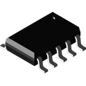
TM1814 is four channels LED constant current adjustable driver IC with function of internal control synchronizing, which can achieve a wide range of display as MCU inputs one group of data set by constant current and PWM to TM1814. When input signal is disconnected, it can realize synchronized fixation of colorful pattern change and prevent in-operation of subsequent cascade chip caused by chip damage. Internal chip is integrated with MCU solidification program and single wire digital interface, data flip-latch, LED constant current driver, circuit, etc. Internal VDD pin is integrated with 5V regulator with less peripheral devices, which applies to guardrail tube, point source and LED decorative products. This product has excellent performance and reliable quality. Features Adopt power CMOS technology Withstand voltage of OUT output port is 32V 5 V voltage-regulator tube is built into VDD, and the voltage supports 6-24 V after cascading the resistor Constant current can achieve level 64 adjustment (6.5 mA-38mA) PWM brightness controls circuit, and 256 brightness is adjustable Accurate current output value Maximum error (between channels): ±3% Maximum error (between chips): ±5% Single line serial concatenated port Oscillation mode: build in RC vibration and conduct clock synchronization according to signals on data line. After receiving the data from this unit, it can reproduce follow-up data and send it to lower level through data output end, and signals will not be distorted and reduced along with cascade Build in power on reset circuit, and after powering on reset, all registers are initialized to zero External control mode data transmission rate is 800 KHZ Internal control mode data transmission rate is 500 KHZ Internal control mode chip sends 2048 points of data Encapsulation mode: SOP8 #CommonPartsLibrary #IntegratedCircuit
0 Uses0 Stars