Interface ICs
An interface IC is a type of integrated circuit that is designed to facilitate communication between two devices or systems. These devices are commonly used in electronic systems to enable the transfer of data and control signals between different components or subsystems. Some common use cases for interface ICs include connecting microcontrollers to peripherals such as sensors or displays, linking multiple processors together in a network, and enabling communication between devices using different communication protocols. Flux.ai has the world's largest community-driven public library of interface ICs, with footprints, symbols, datasheets, and simulation models. This library is a valuable resource for engineers and designers who need access to accurate and up-to-date information on these important components. Whether you are working on a new design project or simply looking to learn more about interface ICs, Flux.ai is an excellent resource to help you find the information you need.
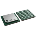
ADC09SJ1300AAVT
Analog to Digital Converters - ADC Single-channel, 9-bit, 1.3-GSPS analog-to-digital converter (ADC) with JESD204C interface 144-FCBGA -40 to 85 ADC09xJ1300 is a family of quad, dual and single channel, 9-bit, 1.3GSPS analog-to-digital converters (ADC). Low power consumption, high sampling rate and 9-bit resolution makes the ADC09xJ1300 ideally suited for suited for a variety of multi-channel communications and test systems. Full-power input bandwidth (-3dB) of 6GHz enables direct RF sampling of L-band and S-band. A number of clocking features are included to relax system hardware requirements, such as an internal phase-locked loop (PLL) with integrated voltagecontrolled oscillator (VCO) to generate the sampling clock. Four clock outputs are provided to clock the logic and SerDes of the FPGA or ASIC. A timestamp input and output is provided for pulsed systems. JESD204C serialized interface decreases system size by reducing the amount of printed circuit board (PCB) routing. Interface modes support from 2 to 8 lanes (dual and quad channel devices) or 1 to 4 lanes (for the single channel device), with SerDes baud-rates up to 17.16Gbps, to allow the optimal configuration for each application. Features • ADC Core: – Resolution: 9 Bit – Maximum sampling rate: 1.3GSPS – Non-interleaved architecture – Internal dither reduces high-order harmonics • Performance specifications (–1dBFS): – SNR (100 MHz): 53.5dBFS – ENOB (100 MHz): 8.5 Bits – SFDR (100 MHz): 64dBc – Noise floor (–20dBFS): –143dBFS • Full-scale input voltage: 80 mVPP-DIFF • Full-power input bandwidth: 6GHz • JESD204C Serial data interface: – Support for 2 to 8 (Quad/Dual channel) or 1 to 4 (Single channel) total SerDes lanes – Maximum baud-rate: 17.16Gbps – 64B/66B and 8B/10B encoding modes – Subclass-1 support for deterministic latency – Compatible with JESD204B receivers • Optional internal sampling clock generation – Internal PLL and VCO (7.2–8.2GHz) • SYSREF Windowing eases synchronization • Four clock outputs simplify system clocking – Reference clocks for FPGA or adjacent ADC – Reference clock for SerDes transceivers • Timestamp input and output for pulsed systems • Power consumption (1GSPS): – Quad Channel: 450mW / channel – Dual channel: 625mW / channel – Single channel: 940mW • Power supplies: 1.1V, 1.9V #CommonPartsLibrary #IntegratedCircuit #ADC #HighSpeedADC #RFADC #JESD204C #13GSPS #9bitADC #DirectRFSampling #TexasInstruments #MixedSignal #DataAcquisition #JESD204
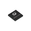
0 Uses0 StarsSTN1110-I/MM
STN1110-IMM General Description The STN1110-IMM is a multiprotocol OBD-II to UART interpreter integrated circuit designed for automotive diagnostic, telematics, and vehicle communication applications. The device translates OBD-II network traffic into a UART serial data stream for communication with external microcontrollers, embedded processors, and host systems. It supports all legislated OBD-II protocols and provides compatibility with ELM327-based software while offering enhanced processing performance, expanded memory resources, advanced message filtering, firmware upgrade capability, and low-power operation. The device is intended for use in automotive diagnostic tools, fleet management systems, vehicle monitoring equipment, data acquisition systems, and embedded automotive communication products. Engineering Specification Part Number: STN1110-IMM Component Type: OBD-II to UART Interpreter Integrated Circuit Device Category: Automotive Communication Interface IC Package Type: QFN Mounting Type: Surface Mount Device (SMD) Interface Type: * UART * OBD-II Supported Protocols: * ISO 15765-4 CAN * ISO 14230-4 KWP2000 * ISO 9141-2 * SAE J1850 PWM * SAE J1850 VPW Key Features: * Multiprotocol OBD-II support * ELM327 command compatibility * Enhanced ST command extensions * High-speed UART communication * Advanced message filtering * Firmware upgrade capability * Large message buffering * Low-power operation * Automotive diagnostic interface functionality Applications: * OBD-II Scan Tools * Vehicle Diagnostics * Automotive Telematics * Fleet Management Systems * Data Logging Equipment * Embedded Automotive Controllers * Emissions Monitoring Systems * Vehicle Communication Gateways Tags #commonpartslibrary #integratedcircuit #ic #automotive #automotiveelectronics #automotivediagnostics #obdii #obd #uart #vehiclecommunication #telematics #embeddedsystems #communicationinterface #diagnosticinterface #scantool #canbus #kwp2000 #saej1850 #iso9141 #surfaceMount #smd #qfn #electroniccomponent #semiconductor #vehicleelectronics #microcontrollerinterface #datalogging #fleetmanagement #embeddedhardware #hardwaredesign
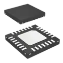
4 Uses0 StarsADS1293CISQ/NOPB
3 Channel AFE 24 Bit 28-WQFN (5x5) ADS1293CISQ/NOPB is a highly integrated, low-power 3-channel ECG Analog Front-End (AFE) from Texas Instruments. It is designed for portable and battery-powered medical devices, fitness monitors, heart-rate monitoring systems, Holter monitors, and other electrocardiogram (ECG) applications. The device integrates signal acquisition, filtering, lead-off detection, right-leg drive generation, and high-resolution analog-to-digital conversion into a single IC, reducing external component count and system cost. Key Features Three high-resolution ECG acquisition channels 24-bit analog-to-digital conversion Simultaneous pace detection support Ultra-low power consumption of approximately 0.3 mW per channel Low input-referred noise of 7 µVpp (40 Hz bandwidth) Programmable sample rates up to 25.6 ksps Differential input voltage range of ±400 mV Integrated EMI-hardened input filters Flexible input routing matrix Built-in Right-Leg Drive (RLD) amplifier AC and DC lead-off detection Integrated Wilson and Goldberger terminal generation Battery voltage monitoring capability Internal oscillator and voltage reference ALARMB pin for interrupt-driven diagnostics and fault reporting Multiple power-down and standby modes for battery-powered systems SPI-compatible digital interface Operating temperature range: –20°C to +85°C 28-pin WQFN package (5 mm × 5 mm) Typical Applications Portable 1-, 3-, 5-, 6-, 7-, 8-, and 12-lead ECG systems Holter monitors Event recorders Telemedicine devices Patient vital-sign monitoring equipment Automated External Defibrillators (AEDs) Sports and fitness heart-rate monitors Wearable medical devices Hashtags #commonpartslibrary #integratedcircuit #TexasInstruments #ADS1293 #AFE #AnalogFrontEnd #ECG #Electrocardiogram #MedicalElectronics #HealthTech #WearableDevices #HeartRateMonitor #PatientMonitoring #BiomedicalEngineering #24BitADC #LowPowerDesign #SPI #SignalConditioning #PortableMedicalDevices #HolterMonitor #Telemedicine #VitalSignsMonitoring #EmbeddedSystems #MixedSignalIC #WQFN28 #BatteryPoweredDevices #MedicalInstrumentation
3 Uses0 StarsPCA9450CHNY
Power Management IC for iMX8M 5V 6A 6 Buck + 5 LDO The PCA9450CHNY is a highly integrated Power Management Integrated Circuit (PMIC) from NXP Semiconductors, specifically designed to power the i.MX 8M family of application processors, particularly the i.MX 8M Plus. It integrates multiple high-efficiency DC-DC buck converters, LDO regulators, power sequencing logic, load switching, voltage monitoring, and system control functions into a single device. The PCA9450C variant features a configurable dual-phase 6 A buck regulator for powering high-current processor cores while supporting Dynamic Voltage Scaling (DVS) for optimized power efficiency. Key Features Six high-efficiency switching regulators (Buck converters) PCA9450C variant supports a configurable 6 A dual-phase buck regulator Three 3 A buck regulators with Dynamic Voltage Scaling (DVS) Remote-sense capability on major buck outputs for IR-drop compensation Five integrated LDO regulators Supports DDR4, LPDDR4, and DDR3L memory configurations 400 mA load switch with active discharge Dual-channel logic level translator Integrated 32.768 kHz crystal oscillator driver Fast-mode Plus (Fm+) 1 MHz I²C interface Programmable power sequencing and voltage control Power ON/OFF and Standby/Run mode control inputs Protection features including UVLO, thermal shutdown, fault monitoring, and soft-start Operating temperature range: −40°C to +105°C 56-pin HVQFN package (7 mm × 7 mm, 0.4 mm pitch) Optimized for i.MX 8M Mini, Nano, and Plus processors, especially the i.MX 8M Plus for the PCA9450C variant. #CommonPartsLibrary #PCA9450CHNY #PCA9450C #NXP #PMIC #PowerManagementIC #PowerSupply #VoltageRegulator #BuckConverter #LDO #DynamicVoltageScaling #DVS #IMX8M #IMX8MPlus #EmbeddedSystems #IndustrialElectronics #PowerManagement #HVQFN56 #Semiconductor #IntegratedCircuit #IC #CommonPartsLibrary #ElectronicsDesign #HardwareDesign #PCBDesign #EmbeddedLinux #IoT #ProcessorPowerManagement #PowerSequencing #SystemPower #NXPSemiconductors
11 Uses0 StarsMT53E1536M32D4DT-046 WT:A
SDRAM - Mobile LPDDR4 Memory IC 48Gbit 2.133 GHz MT53E1536M32D4DT-046 WT:A is a high-density 48Gb (6GB) LPDDR4/LPDDR4X SDRAM memory device from Micron Technology. It is designed for high-performance, low-power applications requiring fast memory bandwidth and efficient power management. The device features a 32-bit data bus, supports data rates up to 4266 MT/s, and is packaged in a compact 200-ball FBGA, making it suitable for embedded computing, industrial systems, networking equipment, AI edge devices, automotive electronics, and mobile platforms. Key Features 48Gb (6GB) LPDDR4/LPDDR4X SDRAM Organized as 1.5G × 32 bits Data transfer rates up to 4266 MT/s Maximum clock frequency of 2133 MHz Low-power operation with 1.1V core supply 32-bit memory interface 200-ball FBGA package JEDEC LPDDR4-compliant architecture Per-bank refresh support Temperature-compensated refresh Self-refresh and deep power-down modes Partial-array self-refresh capability High bandwidth with reduced power consumption Optimized for compact embedded designs Operating temperature range: –30°C to +85°C Typical Applications Embedded Linux computers Single-board computers (SBCs) AI and edge computing platforms Industrial automation systems Networking and telecommunications equipment Automotive infotainment and control systems Tablets and mobile devices FPGA and SoC-based designs #commonpartslibrary #integratedcircuit #memory #dram #sdram #lpddr4 #lpddr4x #mobiledram #micron #embeddedsystems #embeddedcomputing #industrialelectronics #automotiveelectronics #edgecomputing #artificialintelligence #networking #telecommunications #highspeedmemory #lowpowerdesign #computerhardware #electroniccomponents #semiconductor #datasheet #fbga #memorychip #electronicsdesign #pcbdesign #hardwareengineering #electronicengineering #systemonchip #fpga #iot #internetofthings #computermemory #digitalelectronics #surfaceMount #smt #bga #storage #highperformancecomputing #hpc #mobiledevices #industrialautomation #electronicdesign #componentlibrary #fluxlibrary #parametricpart #eda #schematic #pcb #electronicdesignautomation #chipdesign #embeddedhardware #memorymodule #lowpowerelectronics #highbandwidthmemory #electronics #hardwaredevelopment #engineering #electricalengineering
1 Uses0 StarsLRTBGWSR-4U4V-JW+8A8B-D8-3S4U-7Z
Red, Green, Blue (RGB) 626nm Red, 528nm Green, 465nm Blue LED Indication - Discrete 2.15V Red, 2.65V Green, 2.85V Blue 6-PLCC The LRTBGWSR-4U4V-JW+8A8B-D8-3S4U-7Z is an automotive-grade RGB surface-mount LED from the OSIRE® E3635 family by ams OSRAM. It integrates independently controllable red, green, and blue LED chips within a compact 6-PLCC package, enabling precise color mixing and dynamic lighting effects. The device is designed for high-reliability applications requiring full-color illumination, status indication, ambient lighting, and display backlighting. Its wide viewing angle, high luminous intensity, and AEC-Q102 qualification make it suitable for automotive interior lighting, industrial controls, consumer electronics, and advanced human-machine interface applications. Features - Package: white PLCC-6 package, silicone resin - Chip technology: Thinfilm / Volume emitter on Sapphire (AlInGaN) - Typ. Radiation: 120° (Lambertian emitter) - Color: λdom = 626 nm (● red); λdom = 528 nm (● true green); λdom = 465 nm (● blue) - Corrosion Robustness Class: 3B - Qualifications: AEC-Q102 Qualified - ESD: 2 kV acc. to ANSI/ESDA/JEDEC JS-001 (HBM, Class 2) Applications - Ambient Lighting - Automotive Aftermarket #CommonPartsLibrary #LED #RGBLED #OSRAM #amsOSRAM #OSIREE3635 #AutomotiveLED #AECQ102 #SMDLED #PLCC6 #IndicatorLED #AmbientLighting #ColorMixing #LRTBGWSR_4U4V_JW_8A8B_D8_3S4U_7Z
6 Uses0 StarsADXL345TCCZ-EP
Accelerometer X, Y, Z Axis ±2g, 4g, 8g, 16g 0.05Hz ~ 1.6kHz 14-LGA (3x5) The ADXL345-EP is an extended performance version of the ADXL345, which is a small, thin, ultralow power, 3-axis accelerometer with high resolution (13-bit) measurement at up to ±16 g. Digital output data is formatted as 16-bit twos complement and is accessible through either a SPI (3- or 4-wire) or I2 C digital interface. The ADXL345-EP is well suited for extended temperature range industrial and aerospace equipment. It measures the static acceleration of gravity in tilt-sensing applications, as well as dynamic acceleration resulting from motion or shock. Its high resolution (3.9 mg/LSB) enables measurement of inclination changes less than 1.0°. Several special sensing functions are provided. Activity and inactivity sensing detect the presence or lack of motion by comparing the acceleration on any axis with user-set thresholds. Tap sensing detects single and double taps in any direction. Freefall sensing detects if the device is falling. These functions can be mapped individually to either of two interrupt output pins. An integrated memory management system with a 32-level first in, first out (FIFO) buffer can be used to store data to minimize host processor activity and lower overall system power consumption. Low power modes enable intelligent motion-based power management with threshold sensing and active acceleration measurement at extremely low power dissipation. The ADXL345-EP is supplied in a small, thin, 3 mm × 5 mm × 1 mm, 14-lead, enhanced plastic package. Ultralow power: as low as 23 µA in measurement mode and 0.1 µA in standby mode at VS = 2.5 V (typical) Power consumption scales automatically with bandwidth User-selectable resolution from 10 to 13 bits 4 mg/LSB scale factor in all g ranges 32-sample FIFO minimizes host processor load Single tap, double tap, and free-fall detection Activity/inactivity monitoring Supply voltage range: 2.0 V to 3.6 V I/O voltage range: 1.7 V to VS SPI (3- and 4-wire) and I2C digital interfaces Flexible interrupt modes mappable to either interrupt pin Measurement ranges selectable via serial command Bandwidth selectable via serial command 10,000 g shock survival Pb free/RoHS compliant Small and thin: 3 mm × 5 mm × 1 mm LGA package #CommonPartsLibrary #Sensor #Motion-sensor #accelerometer
49 Uses0 StarsBG95M3LA-64-SGNS
Cellular, Navigation BeiDou, EGDE, Galileo, GLONASS, GPS, GNSS, GSM, LTE Transceiver Module 850MHz, 900MHz, 1.8GHz, 1.9GHz Antenna Not Included Surface Mount The BG95M3LA-64-SGNS is a compact low-power LTE cellular communication module designed for IoT, telematics, asset tracking, industrial automation, and embedded wireless applications. The module supports global LTE Cat M1, Cat NB2, and EGPRS connectivity, enabling reliable wide-area wireless communication for battery-powered and mobile embedded systems. The device integrates cellular modem functionality, GNSS positioning capability, power management features, and multiple peripheral communication interfaces within a highly compact surface-mount package optimized for space-constrained embedded designs. The module is engineered for low-power operation, making it suitable for long-life IoT deployments requiring efficient wireless connectivity. The BG95M3LA-64-SGNS supports integrated satellite positioning technologies including GPS, GLONASS, Galileo, and BeiDou for location-aware applications. Its robust RF performance and industrial-grade operating capability allow deployment in harsh environmental conditions and demanding remote monitoring systems. The module provides comprehensive support for embedded communication protocols and is commonly used in smart meters, telematics units, industrial gateways, environmental monitoring systems, fleet tracking devices, and connected sensor platforms. Key Features LTE Cat M1 cellular communication support LTE Cat NB2 narrowband IoT capability EGPRS fallback connectivity Integrated GNSS positioning functionality Low-power optimized architecture Global wireless network compatibility Compact surface-mount module design Embedded TCP/IP protocol stack support UART, USB, and serial communication interfaces Integrated power management subsystem Industrial operating temperature support Embedded IoT connectivity optimization High-reliability wireless communication platform Multi-constellation satellite navigation support Electrical Characteristics Low operating power consumption Wide input voltage support High RF sensitivity performance Embedded low-power sleep functionality Stable wireless communication architecture Integrated RF and baseband processing Optimized antenna interface support Industrial-grade reliability performance Fast network registration capability Applications IoT and M2M communication systems Asset tracking devices Fleet management platforms Smart utility metering Industrial automation equipment Remote environmental monitoring Smart agriculture systems Telematics and transportation electronics Portable wireless data terminals Embedded gateway systems Smart city infrastructure Connected sensor platforms Package Information Package Type: LGA Module Mounting Type: Surface Mount Compact embedded wireless module package RoHS compliant configuration available #commonpartslibrary #wirelessmodule #lte #iot #embeddedhardware #cellularcommunication #gnss #telematics #industrialautomation #assettracking
132 Uses0 StarsRP2040
133MHz LQFN-56(7x7) Microcontrollers (MCU/MPU/SOC) ROHS RP2040 The RP2040 is a high-performance, low-cost 32-bit microcontroller developed by Raspberry Pi Ltd.. It features dual ARM Cortex-M0+ processor cores, flexible digital interfaces, and a unique Programmable I/O (PIO) subsystem that enables custom hardware protocols and timing-critical applications. The device is widely used in embedded systems, IoT devices, robotics, industrial control, consumer electronics, and educational projects. Key Features Dual ARM Cortex-M0+ CPU cores operating up to 133 MHz (up to 200 MHz under specific conditions) 264 KB on-chip SRAM organized in six independent memory banks External QSPI Flash interface with Execute-In-Place (XIP) support and up to 16 MB Flash memory capability 30 multifunction GPIO pins with extensive peripheral multiplexing 2 × UART interfaces 2 × SPI controllers 2 × I²C controllers 16 PWM channels for motor control and signal generation USB 1.1 Host and Device support with integrated PHY 12-bit ADC with four external analog inputs and internal temperature sensor, up to 500 ksps sampling rate 12-channel DMA controller for efficient data transfers Programmable I/O (PIO) subsystem with 8 state machines for implementing custom communication interfaces and precise timing applications Integrated PLLs and programmable LDO regulator for clock and power management Operating voltage range: 1.8 V to 3.3 V Available in a compact 7 mm × 7 mm QFN-56 package Typical Applications IoT and connected devices Industrial automation Robotics and motor control Human-machine interfaces (HMI) Consumer electronics USB peripherals Sensor data acquisition systems Educational and maker projects Custom communication protocol implementations using PIO #CommonPartsLibrary #IntegratedCircuit #Microcontroller
160 Uses0 StarsMAX31865AAP+T
15Bit 3V~3.6V SPI SSOP-20-208mil Analog to Digital Converters (ADCs) ROHS The MAX31865 is an easy-to-use resistance-to-digital converter optimized for platinum resistance temperature detectors (RTDs). An external resistor sets the sensitivity for the RTD being used and a precision delta-sigma ADC converts the ratio of the RTD resistance to the reference resistance into digital form. The MAX31865’s inputs are protected against overvoltage faults as large as Q45V. Programmable detection of RTD and cable open and short conditions is included. ● Integration Lowers System Cost, Simplifies Design Efforts, and Reduces Design Cycle Time • Simple Conversion of Platinum RTD Resistance to Digital Value • Handles 100Ω to 1kΩ (at 0°C) Platinum RTDs (PT100 to PT1000) • Compatible with 2-, 3-, and 4-Wire Sensor Connections • SPI-Compatible Interface • 20-Pin TQFN and SSOP Packages ● High Accuracy Facilitates Meeting Error Budgets • 15-Bit ADC Resolution; Nominal Temperature Resolution 0.03125NC (Varies Due to RTD Nonlinearity) • Total Accuracy Over All Operating Conditions: 0.5NC (0.05% of Full Scale) max • Fully Differential VREF Inputs • 21ms (max) Conversion Time ● Integrated Fault Detection Increases System Reliability • ±45V Input Protection • Fault Detection (Open RTD Element, RTD Shorted to Out-of-Range Voltage, or Short Across RTD Element) #CommonPartsLibrary #IntegratedCircuit #PowerManagement
202 Uses0 Stars