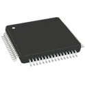
Interface ICs
An interface IC is a type of integrated circuit that is designed to facilitate communication between two devices or systems. These devices are commonly used in electronic systems to enable the transfer of data and control signals between different components or subsystems. Some common use cases for interface ICs include connecting microcontrollers to peripherals such as sensors or displays, linking multiple processors together in a network, and enabling communication between devices using different communication protocols. Flux.ai has the world's largest community-driven public library of interface ICs, with footprints, symbols, datasheets, and simulation models. This library is a valuable resource for engineers and designers who need access to accurate and up-to-date information on these important components. Whether you are working on a new design project or simply looking to learn more about interface ICs, Flux.ai is an excellent resource to help you find the information you need.
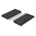
MCP4461-103E/ST
Digital Potentiometer 10k Ohm 4 Circuit 257 Taps I2C Interface 20-TSSOP # Engineering Specification ## Product Name MCP4461-103E/ST ## General Description MCP4461-103E/ST is a non-volatile digital potentiometer integrated circuit designed to provide electronically programmable resistance adjustment for analog and mixed-signal applications. The device enables precise digital control of resistance values through a serial communication interface, eliminating the need for manual potentiometer adjustments and enhancing system automation capabilities. The component integrates multiple resistor networks, non-volatile memory, and digital control logic within a compact package, making it suitable for signal conditioning, gain adjustment, calibration, offset trimming, volume control, and configuration management applications. The design supports reliable operation in embedded systems, industrial electronics, instrumentation equipment, communication devices, and consumer products requiring programmable analog control. The device is optimized for ease of integration, low power consumption, repeatable performance, and long-term reliability. Non-volatile memory functionality allows resistance settings to be retained during power interruptions, supporting consistent system behavior and simplified startup configuration. ## Functional Requirements ### Digital Resistance Control The device shall provide programmable resistance adjustment through a digital communication interface. ### Non-Volatile Memory Operation The device shall retain programmed resistance settings when power is removed and restore stored values upon power-up. ### Multi-Channel Adjustment The device shall support independent control of multiple resistance channels for flexible system configuration. ### Analog Signal Conditioning The device shall support use in gain control, calibration, bias adjustment, offset correction, and signal tuning applications. ## Electrical Requirements ### Power Supply Compatibility The device shall operate from standard low-voltage electronic power supply rails suitable for embedded and industrial systems. ### Digital Communication The device shall support serial communication for configuration, programming, and control of internal resistance networks. ### Resistance Network Performance The device shall provide repeatable and stable resistance adjustment characteristics throughout normal operating conditions. ### Low Power Operation The device shall minimize power consumption while maintaining functional performance and memory retention capability. ### Noise and Signal Integrity The design shall support accurate analog signal processing with minimal impact on system performance. ## Mechanical Requirements ### Package Construction The component shall be supplied in a surface-mount package suitable for automated PCB assembly processes. ### Board Integration The device shall support standard printed circuit board mounting practices and electronic manufacturing workflows. ### Structural Reliability The package shall maintain electrical and mechanical integrity during handling, assembly, and operational service. ## Environmental Requirements ### Operating Environment The device shall operate reliably within environmental conditions commonly encountered in commercial and industrial electronic equipment. ### Storage Conditions The component shall maintain functional and physical integrity during storage, transportation, and inventory management activities. ### Environmental Robustness The design shall support stable operation under expected temperature and humidity variations within specified application environments. ## Quality Requirements ### Reliability The device shall provide consistent long-term performance with stable resistance characteristics and memory retention capability. ### Verification Electrical functionality, communication performance, memory operation, and resistance adjustment behavior shall be validated through applicable testing procedures. ### Compliance The product shall conform to relevant semiconductor manufacturing, quality assurance, and electronic component standards. ## Documentation Requirements Technical documentation shall include device functionality, communication interface requirements, programming guidelines, application recommendations, electrical characteristics, package information, and reliability considerations. ## Classification Tags #MCP4461 #MCP4461103EST #DigitalPotentiometer #NonVolatileMemory #IntegratedCircuit #ICComponent #AnalogElectronics #MixedSignalDesign #SignalConditioning #GainControl #CalibrationCircuit #EmbeddedSystems #ElectronicComponents #ElectricalEngineering #PCBDesign #CircuitDesign #IndustrialElectronics #Instrumentation #CommonPartsLibrary #EngineeringSpecification #ComponentLibrary #TechnicalDocumentation #SystemIntegration #HardwareDevelopment #ReliabilityEngineering
1 Uses0 StarsVIPERGAN65DTR
Converter Offline Flyback Topology 240kHz 16-SO VIPERGAN65DTR is a high-performance engineered system designed for reliable operation in demanding industrial and technical environments. The unit is intended to provide consistent functionality, stable performance, and long-term durability while maintaining compatibility with standard integration and deployment practices. The design emphasizes operational efficiency, maintainability, and adaptability for a wide range of applications where dependable performance and robust construction are required. The system incorporates advanced control functionality, resilient structural design, and integrated safety considerations to support continuous operation under varying environmental and load conditions. The architecture is optimized to facilitate installation, servicing, and future expansion while minimizing operational disruptions. Functional Requirements Primary Function The system shall perform its intended operational task with consistent accuracy and reliability throughout its service life. Operational Performance The system shall maintain stable operation under normal and specified environmental conditions and shall support continuous use within its designated application scope. Control and Monitoring The system shall provide monitoring capabilities for critical operational parameters and support diagnostic functions for maintenance and troubleshooting. Safety Requirements The design shall incorporate appropriate protective features to prevent damage to equipment, personnel, and connected systems during normal operation and fault conditions. Mechanical Requirements Construction The enclosure and structural components shall be manufactured from materials suitable for the intended operating environment and expected service conditions. Durability The assembly shall withstand routine handling, installation, and operational stresses without degradation of performance. Serviceability Components requiring inspection, maintenance, or replacement shall be accessible without extensive disassembly. Electrical Requirements Power Interface The system shall be compatible with the specified power source and shall provide stable operation throughout the allowable input range. Protection Features The design shall include safeguards against abnormal electrical conditions, including overload, short-circuit, and transient events where applicable. Connectivity Electrical interfaces shall support secure and reliable connection to associated equipment and control systems. Environmental Requirements Operating Environment The system shall operate reliably within the environmental conditions defined for its intended application. Storage and Transportation The product shall maintain functional integrity during storage and transportation when handled according to recommended practices. Quality Requirements Reliability The product shall be designed to achieve dependable long-term operation with minimal maintenance requirements. Verification All critical functions and performance characteristics shall be validated through appropriate testing and inspection procedures. Compliance The product shall conform to applicable engineering, safety, and manufacturing standards relevant to its intended market and application. #VIPERGAN65DTR #EngineeringSpecification #CommonPartsLibrary #IntegratedCircuit #ElectronicDesign #HardwareDevelopment #PCBDesign #SystemArchitecture #ComponentLibrary #ElectricalEngineering #EmbeddedSystems #DesignStandard #ProductDevelopment #ManufacturingReady #TechnicalDocumentation #ReliabilityEngineering #IndustrialAutomation #ControlSystem #EngineeringData #ConfigurationManagement #DesignVerification
0 Uses0 StarsADS8688W
16-bit, 500-kSPS, eight-channel, single-supply SAR ADC with ±12-V differential inputs The ADS8684W and ADS8688W are 4-channel and 8-channel, integrated data acquisition systems based on a 16-bit successive approximation (SAR) analogto-digital converter (ADC), operating at a throughput of 500kSPS. The devices feature integrated analog front-end circuitry for each input channel with overvoltage protection up to ±20V, a 4-channel or 8-channel multiplexer with automatic and manual scanning modes, and an on-chip, 4.096V reference with low temperature drift. Operating on a single 5V analog supply, each input channel on the devices can independently support bipolar input ranges of ±12.288V, ±6.144V, and ±3.072V and unipolar input ranges of 12.288V to 0V and 6.144V to 0V. The ADS8684W and ADS8688W offer a simple SPIcompatible serial interface to the digital host and also support daisy-chaining of multiple devices. The digital supply operates from 1.65V to 5.25V, enabling direct interface to a wide range of host controllers Features • 16-Bit ADCs with Integrated Analog Front-End • 4-, 8-Channel MUX with Auto and Manual Scan • Channel-Independent Programmable Inputs: – ±12.288V, ±6.144V, and ±3.072V – 12.288V to 0V and 6.144V to 0V • 5V Analog Supply: 1.65V to 5V I/O Supply • Constant Resistive Input Impedance: 1.2MΩ • Input Overvoltage Protection: Up to ±20V • On-Chip, 4.096V Reference with Low Drift • Excellent Performance: – 500kSPS Aggregate Throughput – DNL: ±0.6LSB; INL: ±0.8LSB – Low Drift for Gain Error and Offset – SNR: 91.5dB; THD: –102dB – Low Power: 65mW • AUX Input → Direct Connection to ADC Inputs • ALARM → High and Low Thresholds per Channel • SPI™-Compatible Interface with Daisy-Chain • Industrial Temperature Range: –40°C to 125°C #commonpartslibrary #ADS8688W #TexasInstruments #ADC #SARADC #DataAcquisition #IndustrialAutomation #SPI #PrecisionADC #AnalogFrontEnd #EmbeddedSystems #MeasurementSystems
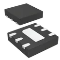
34 Uses0 StarsMAX44009EDT+T
Optical Sensor Ambient I2C 6-UDFN Exposed Pad ## Engineering Specification ## General Description The **MAX44009EDT+T** is an Analog Devices / Maxim Integrated digital ambient light sensor designed for portable electronics, display brightness control, industrial sensors, embedded systems, and low-power optical sensing applications. It integrates an ambient light photodiode, signal conditioning, analog-to-digital conversion, and an I²C digital output interface in a compact surface-mount package. The device is suitable for systems requiring automatic brightness adjustment, low current consumption, and light measurement behavior that closely follows human-eye response. ## Device Identification Manufacturer Part Number: **MAX44009EDT+T** Manufacturer: **Analog Devices / Maxim Integrated** Product Series: **MAX44009** Device Category: **Sensor Integrated Circuit** Device Type: **Digital Ambient Light Sensor** Sensor Interface: **I²C Digital Output** Mounting Type: **Surface Mount** Package Type: **UTDFN-Opto / UDFN** ## Functional Description The device functions as a digital ambient light sensor that measures surrounding light intensity and reports the measurement through an I²C interface. It is designed to help electronic systems adjust display brightness, conserve power, improve user visibility, and respond to changes in lighting conditions. The integrated optical sensing and digital conversion circuitry reduce the need for external analog signal-conditioning components. ## Optical Sensing Description The sensor includes an on-chip photodiode with spectral response optimized to approximate human-eye sensitivity. It also incorporates infrared and ultraviolet blocking capability to improve ambient light measurement accuracy. The adaptive gain function automatically selects the appropriate measurement range, allowing the device to operate across very low-light and bright-light conditions. ## Electrical Description The **MAX44009EDT+T** operates from a low-voltage supply range and is optimized for ultra-low power consumption. It supports digital communication through an I²C interface and is suitable for battery-powered and energy-sensitive systems. Proper supply decoupling, pull-up resistor selection, and bus voltage compatibility should be considered during circuit design. ## Package and Mechanical Description The component is supplied in a compact surface-mount optical package suitable for space-constrained printed circuit board designs. The package is intended for placement where the optical sensing window has access to ambient light while maintaining proper mechanical protection from contamination, shadowing, and enclosure obstruction. ## Interface and Control Description The device communicates with a host microcontroller or processor through an I²C digital interface. The host can read ambient light data and configure device behavior through register-based communication. The selectable I²C addressing feature supports flexible integration in systems that may include multiple I²C peripherals. ## Mounting and Assembly Description The **MAX44009EDT+T** is intended for surface-mount PCB assembly using standard reflow soldering processes. PCB layout should follow the manufacturer’s recommended footprint and assembly guidance. The optical sensing area should remain unobstructed, clean, and aligned with the product enclosure opening or light pipe when used. ## Application Suitability The device is suitable for smartphones, tablets, notebooks, wearable electronics, handheld devices, display brightness control, industrial light sensing, smart home devices, battery-powered equipment, sensor modules, and embedded systems requiring digital ambient light detection. ## Design Considerations The design should account for sensor placement, optical window design, enclosure transparency, light pipe geometry, I²C bus pull-up values, supply voltage compatibility, ambient interference, temperature conditions, and contamination protection. The sensor should not be blocked by opaque materials or placed where shadows, reflections, or nearby LEDs may distort the measured ambient light level. ## Hashtags #commonpartslibrary #integratedcircuit #sensor #ambientlightsensor #digitalsensor #opticalsensor #analogdevices #maximintegrated #max44009 #max44009edt #i2csensor #lightmeasurement #brightnesscontrol #lowpowersensor #portableelectronics #displaycontrol #embeddedhardware #embeddeddesign #smdcomponent #surfacemount #utdfnpackage #uDFNpackage #pcbdesign #hardwaredesign #electronicscomponents #electronicparts #componentlibrary #engineeringparts #electronicsengineering
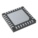
9 Uses0 StarsLAN8770M-I/PRA
4/4 Transceiver Full MII, RMII 32-VQFN (5x5) ## Engineering Specification ## General Description The **LAN8770M-I/PRA** is a Microchip Technology single-port **100BASE-T1 Ethernet physical layer transceiver** designed for automotive, industrial, and embedded networking applications. It provides Ethernet communication over a single balanced twisted pair and is suitable for compact systems requiring reliable network connectivity, low-power operation, and standard MAC interface support. The device is commonly used in automotive electronic control units, infotainment systems, telematics modules, sensor nodes, industrial control systems, and embedded Ethernet hardware. ## Device Identification Manufacturer Part Number: **LAN8770M-I/PRA** Manufacturer: **Microchip Technology** Product Family: **LAN8770** Device Category: **Integrated Circuit** Device Type: **Ethernet PHY Transceiver** Ethernet Standard: **100BASE-T1** Interface Type: **MII and RMII** Mounting Type: **Surface Mount** Package Type: **VQFN** ## Functional Description The device functions as an Ethernet physical layer transceiver that connects a host controller or microcontroller MAC interface to a single-pair Ethernet physical medium. It handles the analog and digital PHY functions required for 100BASE-T1 communication, allowing embedded systems to transmit and receive Ethernet data over a single twisted pair cable. ## Network and Interface Description The **LAN8770M-I/PRA** supports 100 Mb/s single-pair Ethernet communication and provides MII and RMII host interface options. This allows integration with microcontrollers, processors, gateways, and network controllers that support standard Ethernet MAC interfaces. The device is intended for applications where compact Ethernet connectivity and reduced cabling complexity are required. ## Electrical Description The device is designed for low-voltage operation and supports multiple supply domains according to the manufacturer’s recommended operating conditions. Proper power sequencing, decoupling, reset handling, clocking, and reference layout should be implemented to maintain stable PHY operation and signal integrity. ## Package and Mechanical Description The component is supplied in a compact surface-mount **VQFN package**, suitable for dense printed circuit board assemblies. The package supports automated assembly and is appropriate for space-constrained automotive and industrial electronic designs. ## Control and Diagnostic Description The PHY supports management and configuration through standard control interfaces used in Ethernet designs. It provides status monitoring and configuration capability for link management, operating mode selection, and system-level diagnostics. These features allow the host controller to configure and monitor Ethernet link behavior during operation. ## Automotive and Industrial Suitability The **LAN8770M-I/PRA** is suitable for embedded systems requiring robust single-pair Ethernet communication. It is applicable to automotive networking, telematics, infotainment, advanced driver assistance systems, industrial Ethernet nodes, building automation, control modules, and other connected embedded platforms. ## Mounting and Assembly Description The component is intended for surface-mount PCB assembly using standard reflow soldering processes. PCB layout should follow Microchip’s hardware design guidance, including proper power supply decoupling, controlled impedance routing, short signal paths, grounding, and separation of sensitive analog and digital sections where applicable. ## Design Considerations The design should account for Ethernet signal integrity, single-pair cable interface requirements, common-mode noise control, EMC performance, supply filtering, oscillator or clock source requirements, reset timing, thermal performance, and package solderability. The device should not be operated beyond the manufacturer’s specified electrical, thermal, or mechanical limits. ## Application Suitability The device is suitable for automotive Ethernet nodes, electronic control units, telematics modules, infotainment systems, sensor interfaces, industrial controllers, embedded gateways, connected equipment, and compact network-enabled hardware requiring 100BASE-T1 Ethernet PHY functionality. ## Hashtags #commonpartslibrary #integratedcircuit #ethernetphy #microchip #microchiptechnology #lan8770 #lan8770mipra #singlepairethernet #100baset1 #automotiveethernet #ethernettransceiver #phytransceiver #embeddednetworking #mii #rmii #vqfnpackage #smdcomponent #surfacemount #automotiveelectronics #industrialethernet #telematics #infotainment #embeddedhardware #pcbdesign #hardwaredesign #electronicscomponents #electronicparts #componentlibrary #engineeringparts #electronicsengineering
3 Uses0 StarsS32K358GHT1MJBST
ARM® Cortex®-M7 S32K3 Microcontroller IC 32-Bit Tri-Core 240MHz 8MB (8M x 8) FLASH 289-LFBGA (14x14) ## Engineering Specification ## General Description The **S32K358GHT1MJBST** is an NXP Semiconductors **S32K3 series automotive microcontroller** designed for high-performance embedded control applications in automotive, industrial, and electrically harsh environments. It is built around an **Arm Cortex-M7 architecture** and provides high processing capability, large embedded flash memory, automotive-grade qualification, security support, and a broad set of communication interfaces. The device is suitable for body control, gateway systems, vehicle networking, motor control, domain control, safety-related embedded systems, and general-purpose automotive electronic control units. ## Device Identification Manufacturer Part Number: **S32K358GHT1MJBST** Manufacturer: **NXP Semiconductors** Product Family: **S32K3** Device Category: **Integrated Circuit** Device Type: **Automotive Microcontroller** Core Architecture: **Arm Cortex-M7** Processing Class: **Thirty-Two-Bit MCU** Qualification: **Automotive Grade, AEC-Q100** ## Functional Description The device functions as a high-performance automotive microcontroller for embedded control and communication systems. It provides processing resources for real-time control, communication management, diagnostics, security handling, and system-level application logic. The microcontroller is designed for scalable automotive platforms where software reuse, safety capability, and peripheral integration are important. ## Core and Processing Description The **S32K358GHT1MJBST** uses an Arm Cortex-M7 based processing architecture with tri-core capability and high-speed operation. The core architecture supports digital signal processing, floating-point operation, interrupt handling, and real-time embedded software execution. This makes the device suitable for control systems that require strong computing performance and deterministic response. ## Memory Description The device includes large embedded flash memory for application firmware storage and integrated RAM for runtime operation, data buffering, communication stacks, and control algorithms. The memory architecture is suitable for complex embedded applications requiring large program space, diagnostics, bootloader support, and over-the-air update capability. ## Security and Safety Description The microcontroller includes hardware security support through **HSE-B security** and is intended for automotive applications where secure boot, cryptographic services, protected firmware operation, and system integrity are important. The S32K3 family also supports automotive safety-oriented development through features such as error correction, monitoring, and diagnostic capability. ## Communication and Interface Description The device supports multiple embedded communication interfaces suitable for vehicle and industrial networks. Supported interface types include CAN, Ethernet, I²C, SPI, UART, LIN, QSPI, SAI, SENT, and FlexIO. These interfaces allow the device to communicate with sensors, actuators, transceivers, memory devices, network controllers, and other electronic control units. ## Analog and Peripheral Description The microcontroller includes analog-to-digital conversion capability, timers, watchdog functions, direct memory access, serial audio support, and general-purpose input and output resources. These peripherals support sensing, control, timing, supervision, communication, and system management functions in embedded hardware designs. ## Electrical Description The device is designed for automotive low-voltage operation and supports use across a wide supply voltage range. It is intended for applications requiring reliable operation in automotive and industrial temperature environments. Proper power supply design, decoupling, reset control, clock configuration, and grounding should follow the manufacturer’s hardware design recommendations. ## Package and Mechanical Description The **S32K358GHT1MJBST** is supplied in a **surface-mount LFBGA package** with a compact ball-grid-array footprint. The package is intended for dense printed circuit board layouts requiring careful routing, controlled assembly process, thermal management, and proper solder joint reliability. ## Mounting and Assembly Description The component is intended for automated surface-mount PCB assembly using BGA-compatible manufacturing processes. PCB layout should follow the recommended footprint, ball escape routing, power-plane design, decoupling capacitor placement, thermal design, and inspection requirements for high-density automotive microcontroller assemblies. ## Application Suitability The device is suitable for automotive electronic control units, body control modules, gateway controllers, vehicle networking systems, motor control platforms, battery-related control systems, industrial controllers, safety-oriented embedded systems, and high-performance general-purpose control applications. ## Design Considerations The design should account for supply voltage range, clocking requirements, flash and RAM usage, thermal limits, package routing density, communication interface requirements, EMC performance, boot configuration, security provisioning, debugging access, software safety requirements, and compliance with automotive design guidelines. The device should not be operated beyond the manufacturer’s specified electrical, thermal, or mechanical limits. ## Hashtags #commonpartslibrary #integratedcircuit #microcontroller #automotivemcu #nxp #nxpsemiconductors #s32k3 #s32k358 #s32k358ght1mjbst #armcortexm7 #cortexm7 #thirtytwobit #automotiveelectronics #aecq100 #hsesecurity #canfd #ethernet #vehicleelectronics #embeddedhardware #embeddeddesign #ecu #gatewaycontroller #bodycontrolmodule #pcbdesign #hardwaredesign #electronicscomponents #electronicparts #componentlibrary #engineeringparts #electronicsengineering
2 Uses0 Stars1726040
2 Position Wire to Board Terminal Block Horizontal with Board 0.200" (5.08mm) Through Hole ## Engineering Specification ## General Description The **1726040** is a Phoenix Contact **MKKDSN series PCB terminal block** designed for wire-to-board electrical connections in printed circuit board assemblies. It is used to provide a secure screw-clamp interface between external wiring and PCB circuitry. The component is suitable for control systems, industrial electronics, power distribution circuits, automation equipment, and general electronic assemblies requiring reliable field wiring termination. ## Device Identification Manufacturer Part Number: **1726040** Manufacturer: **Phoenix Contact** Product Series: **MKKDSN** Device Category: **Connector and Interconnect Component** Device Type: **PCB Terminal Block** Connection Type: **Wire-to-Board Terminal Block** Mounting Type: **Through-Hole PCB Mount** Termination Method: **Screw Connection** ## Functional Description The device functions as a fixed printed circuit board terminal block that allows external conductors to be connected directly to a PCB. The screw-clamp mechanism secures the wire mechanically and electrically, providing a stable connection for signal or power circuits. The terminal block is intended for applications where field wiring must be removable, serviceable, and mechanically secure. ## Mechanical Description The component uses a compact green housing suitable for PCB-mounted assemblies. It is designed for side-entry conductor connection and horizontal board installation. The terminal block construction supports organized wire routing and convenient access for installation, maintenance, and service work. ## Electrical Description The terminal block is intended for low-voltage power and signal applications within the manufacturer’s specified current and voltage ratings. It provides reliable conductor contact when properly installed with compatible wire sizes and appropriate tightening torque. ## Material and Contact Description The connector housing is typically made from insulating material suitable for electrical safety and PCB assembly use. The internal conductive elements provide the electrical path between the inserted wire and the soldered PCB connection. Proper conductor preparation and screw tightening are required to maintain stable electrical performance. ## Mounting and Assembly Description The component is intended for through-hole solder mounting on a printed circuit board. Proper PCB hole sizing, pad layout, soldering process control, and mechanical clearance should be followed according to the manufacturer’s recommended design and assembly guidance. The terminal block should be mounted in a position that allows safe wire insertion and screw access. ## Application Suitability The **1726040** is suitable for industrial control boards, automation equipment, interface modules, power supply circuits, instrumentation, building control systems, relay boards, sensor wiring interfaces, and other electronic products requiring secure PCB wire termination. ## Design Considerations The design should account for wire gauge compatibility, current rating, voltage rating, tightening torque, creepage and clearance requirements, solder joint strength, and accessibility for field wiring. The terminal block should not be used beyond the manufacturer’s specified electrical, thermal, and mechanical limits. ## Hashtags #commonpartslibrary #terminalblock #pcbterminalblock #phoenixcontact #mkkdsn #wiretoboard #connector #interconnect #fixedterminalblock #screwterminal #throughholecomponent #pcbmount #industrialelectronics #automationequipment #controlsystems #powerdistribution #fieldwiring #electronicscomponents #electronicparts #hardwaredesign #pcbdesign #engineeringparts #componentlibrary #electronicsengineering
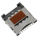
79 Uses0 Stars693022010811
8 Position Card Connector Micro SIM Surface Mount, Right Angle Gold ## Engineering Specification ## General Description The **693022010811** is a Würth Elektronik **WR-CRD Micro SIM card connector** designed for compact electronic devices requiring secure SIM card retention and reliable board-level electrical connection. It is intended for surface-mount printed circuit board assembly and is suitable for communication modules, wireless devices, embedded systems, IoT hardware, and networking equipment. The connector uses a hinged lid mechanism to hold the Micro SIM card in place during operation. ## Device Identification Manufacturer Part Number: **693022010811** Manufacturer: **Würth Elektronik** Product Series: **WR-CRD** Device Category: **Connector and Interconnect Component** Device Type: **Micro SIM Card Connector** Connector Style: **Hinge Type** Mounting Type: **Surface Mount, Right Angle** ## Functional Description The device functions as a board-mounted Micro SIM card interface. It provides mechanical retention and electrical contact between the SIM card and the host printed circuit board. The hinged lid design allows the SIM card to be placed into the connector and secured during operation, helping maintain contact stability in compact electronic assemblies. ## Mechanical Description The connector is designed with a low-profile surface-mount construction suitable for space-constrained PCB layouts. It uses a hinged card-retention mechanism and is intended for horizontal or right-angle card installation. The mechanical structure supports reliable insertion, retention, and removal of the Micro SIM card during normal use. ## Electrical Description The connector is intended for signal-level SIM card interface applications. It provides multiple gold-plated contact positions for stable electrical connection between the SIM card and the host circuit. The device should be used within the manufacturer’s specified voltage, current, contact resistance, and insulation limits. ## Material and Contact Description The connector uses copper alloy contacts with gold plating for reliable signal transfer and corrosion resistance. The housing and mechanical retention structure are designed for surface-mount assembly and repeated card handling within the rated operating conditions. ## Mounting and Assembly Description The component is suitable for automated surface-mount PCB assembly. Proper land pattern design, soldering profile control, and mechanical clearance should be followed according to the manufacturer’s recommended layout and assembly guidance. The PCB design should provide stable grounding, correct pad alignment, and adequate clearance for SIM card insertion and lid operation. ## Application Suitability The **693022010811** is suitable for cellular communication devices, IoT modules, wireless routers, embedded modems, tracking systems, smart meters, industrial communication equipment, portable electronics, and other products requiring a Micro SIM card interface. ## Design Considerations The connector should be placed in an accessible area of the PCB to allow SIM card installation and removal. Designers should avoid excessive mechanical stress on the hinged lid, improper solder joint loading, contamination of the contact area, and operation beyond the specified environmental and electrical ratings. ## Hashtags #commonpartslibrary #connector #simconnector #microsimconnector #wurthelektronik #wrcrd #cardconnector #memoryconnector #interconnect #pcbconnector #surfacemount #rightangleconnector #smtcomponent #goldplatedcontacts #embeddedhardware #iotdevices #wirelessmodules #communicationdevices #networkingequipment #pcbdesign #hardwaredesign #electronicscomponents #electronicparts #componentlibrary #engineeringparts #electronicsengineering
2 Uses0 StarsMSLPT5252AG2TR
Tactile Switch SPST-NO Top Actuated Surface Mount ## Engineering Specification ## General Description The **MSLPT5252AG2TR** is a TE Connectivity ALCOSWITCH low-profile tactile switch designed for compact electronic devices, printed circuit board assemblies, portable electronics, control panels, and user-input interface applications. It provides momentary tactile feedback when pressed and returns to its normal open state when released. The device is suitable for applications requiring a small surface-mount switch with reliable actuation, compact board footprint, and low-profile mechanical construction. ## Device Identification Manufacturer Part Number: **MSLPT5252AG2TR** Manufacturer: **TE Connectivity** Brand Series: **ALCOSWITCH** Product Family: **LPT Low-Profile Tactile Switches** Device Category: **Electromechanical Component** Device Type: **Tactile Switch** Switch Function: **Single Pole Single Throw, Normally Open** ## Functional Description The device functions as a momentary user-input switch. When the actuator is pressed, the internal contacts close and allow an electrical signal path. When the actuator is released, the switch returns to its normally open condition. This makes the component suitable for button input, menu control, reset functions, mode selection, and general human-machine interface designs. ## Mechanical Description The switch uses a compact low-profile construction with a top-actuated flush actuator. It is intended for surface-mount installation on printed circuit boards and is suitable for space-constrained designs where low height and small board area are required. ## Electrical Description The MSLPT5252AG2TR is designed for low-current DC switching applications. It should be used within the manufacturer’s specified voltage and current ratings to ensure reliable operation and long service life. The switch is intended for signal-level control applications rather than high-power load switching. ## Contact and Material Description The switch includes stainless steel contact base material with silver contact plating. This construction supports reliable contact performance for tactile input applications and helps provide stable electrical switching behavior during normal operation. ## Mounting and Assembly Description The component is supplied as a surface-mount tactile switch suitable for automated PCB assembly. Proper land pattern design, soldering profile control, and mechanical clearance should be followed according to the manufacturer’s recommended layout and assembly guidelines. ## Application Suitability The device is suitable for portable electronic devices, consumer electronics, handheld equipment, control buttons, reset switches, interface panels, communication devices, instrumentation, remote controls, and compact PCB-based user-input systems. ## Design Considerations The switch should be placed in a location that allows direct actuator access without excessive mechanical side loading. PCB layout should provide proper solder pad support and mechanical stability. The design should avoid overtravel, excessive actuation force, contamination, and use beyond the rated electrical limits. ## Hashtags #commonpartslibrary #electromechanicalcomponent #tactileswitch #pushbuttonswitch #momentaryswitch #spstswitch #normallyopen #teconnectivity #alcoswitch #mslpt5252ag2tr #lptseries #smtcomponent #surfacemount #pcbdesign #electronicscomponents #electronicparts #switchcomponent #hardwaredesign #userinterface #embeddedhardware #consumer electronics #portableelectronics #componentlibrary #engineeringparts #electronicsengineering
85 Uses0 StarsR7FA6E10F2CFM#AA0
ARM® Cortex®-M33 RA6E1 Microcontroller IC 32-Bit 200MHz 1MB (1M x 8) FLASH 64-LFQFP (10x10) ## Engineering Specification ## General Description The **R7FA6E10F2CFM#AA0** is a Renesas Electronics **RA6E1 series microcontroller** designed for embedded control, industrial electronics, IoT edge devices, automation systems, and general-purpose connected applications. It is built around an **Arm Cortex-M33 processor with TrustZone support**, providing high performance, secure execution capability, and flexible integration for modern embedded designs. ## Device Identification Manufacturer Part Number: **R7FA6E10F2CFM#AA0** Manufacturer: **Renesas Electronics** Product Family: **RA Family** Series: **RA6 Series** Group: **RA6E1 Group** Device Category: **Integrated Circuit** Device Type: **Microcontroller Unit** ## Core and Processing The device uses an **Arm Cortex-M33 core** and is intended for high-performance embedded processing. It supports secure application development through TrustZone technology and is suitable for systems requiring reliable control, fast response, and efficient software execution. ## Memory Configuration The microcontroller includes program flash memory, data flash memory, and SRAM resources suitable for embedded firmware, application code, configuration storage, and runtime processing requirements. ## Package and Mechanical Description The component is supplied in an **LQFP surface-mount package**, making it suitable for compact printed circuit board layouts and standard automated assembly processes. ## Electrical and Operating Description The device is designed for low-voltage embedded systems and supports operation across an industrial temperature range. It is suitable for products requiring stable performance in controlled, commercial, or industrial operating environments. ## Communication and Interface Support The device supports common embedded communication interfaces such as USB, UART, SPI, I²C, QSPI, and CAN, allowing integration with sensors, displays, external memory, communication modules, and other peripheral devices. ## Analog and Control Features The microcontroller includes analog conversion capability, timer functions, PWM support, watchdog protection, reset monitoring, and low-voltage detection features. These functions make it suitable for control systems, monitoring equipment, and mixed-signal embedded applications. ## Security and Debug Features The device supports embedded security functions including TrustZone, unique device identification, and true random number generation. Debug and development access is supported through standard JTAG and SWD interfaces. ## Application Suitability This device is suitable for embedded controllers, IoT devices, industrial automation, metering equipment, appliance control, USB-connected products, sensor-based systems, and general electronic control applications requiring a compact and secure microcontroller solution. ## Hashtags #commonpartslibrary #integratedcircuit #microcontroller #renesas #renesaselectronics #ra6e1 #ra6series #armcortexm33 #embeddedsystems #electronicscomponents #semiconductor #mcu #iotdevices #industrialautomation #pcbdesign #electronicparts #componentlibrary #engineeringparts #hardwaredesign #electronicsengineering
0 Uses0 Stars