Interface ICs
An interface IC is a type of integrated circuit that is designed to facilitate communication between two devices or systems. These devices are commonly used in electronic systems to enable the transfer of data and control signals between different components or subsystems. Some common use cases for interface ICs include connecting microcontrollers to peripherals such as sensors or displays, linking multiple processors together in a network, and enabling communication between devices using different communication protocols. Flux.ai has the world's largest community-driven public library of interface ICs, with footprints, symbols, datasheets, and simulation models. This library is a valuable resource for engineers and designers who need access to accurate and up-to-date information on these important components. Whether you are working on a new design project or simply looking to learn more about interface ICs, Flux.ai is an excellent resource to help you find the information you need.
88615-5005
15 Position D-Sub Plug, Male Pins Connector The 88615-5005 is a D-subminiature connector manufactured by 3M, configured as a plug-style connector with male pin contacts. D-subminiature connectors, commonly known as D-Sub connectors, are among the most widely used and longest-standing rectangular connector standards in the electronics industry, recognized by their characteristic trapezoidal metal shell that provides a self-aligning, polarized mating interface and a degree of mechanical shielding for the contacts housed within. This particular connector is built around a defined male pin contact arrangement housed within the standard D-shaped metal shell, which serves to guide correct mating alignment with its corresponding female socket connector counterpart while also helping to reduce the risk of bent or damaged pins during the mating process. As a plug-style device with pin contacts, this connector is typically mounted on a cable assembly, panel, or enclosure and is intended to mate with a female D-Sub receptacle mounted on a printed circuit board, another cable assembly, or an equipment panel, forming a complete signal or low-power interconnect path between two systems or subsystems. D-Sub connectors of this style have long been used across an extremely broad range of applications, including legacy computer peripheral interfaces, industrial control systems, test and measurement equipment, instrumentation racks, and many other applications requiring a rugged, field-serviceable, and widely interoperable multi-pin connection. Their enduring popularity stems from the connector family's mechanical robustness, ease of hand assembly and field termination, broad availability of compatible mating hardware such as backshells and hoods, and long-established presence in legacy and ruggedized electronic system designs across commercial, industrial, and aerospace sectors. 3M's D-Sub connector assemblies in this product family are typically constructed using a metal or metal-plated shell to provide mechanical strength and a degree of electromagnetic shielding, paired with an insulating housing that holds the individual pin contacts in precise alignment. The pin contacts themselves are typically machined or stamped from a conductive alloy and plated to ensure low-resistance, corrosion-resistant electrical contact across the connector's service life. As is typical for connectors in this product class, the device is intended for general-purpose signal and low-power interconnection rather than high-speed digital or high-current power transmission, making it well suited to control signal routing, instrumentation wiring, and other moderate-density interconnect applications. Spec Sheet Identification Part Number: 88615-5005 Connector Family: D-Sub Connector Assemblies Manufacturer: 3M Connector Type / Configuration Type: D-Subminiature connector Gender: Plug, male pin contacts Contact Style: Male pins Shell Style: Standard D-shaped trapezoidal metal shell Mechanical Specifications Mounting Style: Cable-mount or panel-mount plug configuration Mating Interface: Standard D-Sub polarized shell, self-aligning Contact Material: Conductive alloy pin contacts, plated for corrosion resistance and low contact resistance Application Context Typical Use: General-purpose signal and low-power interconnection Common Applications: Industrial control systems, instrumentation, test and measurement equipment, legacy peripheral interfaces, panel and rack wiring Compatibility Mates With: Corresponding D-Sub female socket receptacle connector Accessory Compatibility: Compatible with standard D-Sub backshells, hoods, and jackscrew hardware Environmental & Qualification Construction Class: General-purpose connector construction typical of the D-Sub product family RoHS Compliance: Per 3M product documentation for this series Packaging Supply Format: Standard connector packaging per 3M distribution practices #88615 #3M #DSubConnector #DSubminiature #ConnectorAssembly #MalePinConnector #PlugConnector #SignalConnector #IndustrialConnector #InstrumentationConnector #PanelMount #CableAssembly #RectangularConnector #ElectronicComponents #PCBDesign #HardwareEngineering #EngineeringSpec #ComponentLibrary #CommonPartsLibrary #ConnectorDatasheet
0 Uses0 StarsTCAN1462DRQ1
1/1 Transceiver Half CANbus 8-SOIC The TCAN1462DRQ1 is an automotive-grade, fault-protected CAN FD transceiver manufactured by Texas Instruments, designed to serve as the physical-layer interface between a CAN protocol controller and the physical CAN bus wiring in a vehicle network. The device meets the physical layer requirements of the high-speed CAN standard and additionally complies with the Signal Improvement Capability specification, a more demanding industry standard developed to address signal integrity challenges that arise in complex, high-node-count automotive network topologies. A central feature of this transceiver is its ability to actively reduce signal ringing that occurs during dominant-to-recessive bus transitions, a phenomenon that becomes increasingly problematic as networks grow larger, bus speeds increase, and more unterminated branch connections are introduced into the topology. By suppressing this ringing, the device allows the network to reliably support higher CAN FD data rates and more complex star or multi-drop topologies than would be achievable with a conventional CAN transceiver, enabling designers to extract the full throughput benefit of the CAN FD protocol even in challenging real-world wiring harness configurations. The device also meets tighter bit-timing symmetry requirements than standard CAN FD transceivers, which widens the timing margin available for correctly sampling each bit and helps prevent communication errors caused by ringing and bit distortion in large, complex networks. This particular part number is pin-compatible with other widely used 8-pin CAN FD transceivers, allowing it to serve as a drop-in upgrade path for existing automotive electronic control unit designs seeking improved signal integrity without requiring a board redesign. The device supports a low-power standby mode that allows the transceiver to enter a reduced-current state while still being able to detect a wake-up pattern transmitted over the bus, supporting remote wake-up functionality that is essential for modern vehicle networks where many control modules must remain dormant but responsive while the vehicle is parked. Robust fault protection is built into the device to support reliable operation in the harsh electrical environment of a vehicle, including comprehensive bus fault protection against high-voltage transients and short circuits, along with internal mechanisms to detect undervoltage conditions, prevent device damage from excessive internal temperature, and guard against a stuck or fault-driven transmit input from indefinitely holding the bus in a dominant state. Together, these protection features allow the transceiver to maintain network integrity even when subjected to electrical faults, wiring harness damage, or unexpected operating conditions common in automotive environments. The device is housed in a small-outline surface-mount package suited to space-constrained automotive electronic control unit designs and is qualified to automotive electronics reliability standards, reflecting its suitability for deployment in body, chassis, powertrain, and infotainment network nodes throughout a vehicle. Spec Sheet Identification Part Number: TCAN1462DRQ1 Device Family: TCAN1462-Q1 Manufacturer: Texas Instruments Functional Classification Device Type: CAN FD transceiver Compliance: High-speed CAN physical layer standard, Signal Improvement Capability (SIC) specification Pin Compatibility: Compatible with standard 8-pin CAN FD transceiver pinouts Signal Integrity Features Ringing Suppression: Active reduction of dominant-to-recessive edge ringing Bit Timing: Tightened bit-timing symmetry for improved sampling margin Supported Topologies: Large, complex networks including star topologies with multiple unterminated stubs Data Rate Support: Enhanced throughput at elevated CAN FD data rates Power & Operating Modes Standby Mode: Low-power standby with bus wake-up pattern detection Wake-Up Compliance: Remote wake-up per high-speed CAN wake-up pattern standard Protection Features Bus Fault Protection: High-voltage bus fault protection Undervoltage Detection: Integrated undervoltage monitoring Thermal Shutdown: Integrated overtemperature protection Driver Timeout: Dominant-state timeout protection on transmit input Environmental & Qualification Temperature Grade: Extended automotive operating temperature range Automotive Qualification: AEC-Q100 qualified Lifecycle Status: Active production Package Package Type: Small-outline surface-mount package (SOIC style) Mounting: Surface mount technology (SMT) Terminal Form: Gull-wing leads Packaging Format Supply Format: Tape-and-reel or cut-tape packaging options #TCAN1462 #TexasInstruments #CANTransceiver #CANFD #AutomotiveIC #AECQ100 #SignalImprovementCapability #VehicleNetworking #InVehicleNetwork #FaultProtected #SOIC #SurfaceMount #AutomotiveElectronics #ECU #SemiconductorIC #EngineeringSpec #ComponentLibrary #CommonPartsLibrary #RoHSCompliant #PhysicalLayerIC
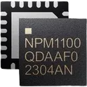
31 Uses0 StarsNPM1100-QDAA-R7
Battery Power Management IC Lithium Ion/Polymer 24-QFN (4x4) nPM1100 is an integrated Power Management IC (PMIC) with a linear-mode lithium-ion/lithium-polymer battery charger in a compact 2.1x2.1 mm WLCSP package. It has a highly efficient, dual-mode configurable output DC/DC buck regulator. nPM1100 is an extremely compact PMIC device, created for space constrained applications with a small lithium-ion or lithium-polymer battery. It is compatible with all nRF52 and nRF53 Series SoCs and supports charging batteries at up to 500 mA through USB, and also delivers up to 150 mA of current to power external components with regulated voltage. A minimum of five passive components are required for operation and the device functions without a control interface. It is the perfect companion for nRF52 and nRF53 multiprotocol SoCs in battery powered designs. Low quiescent current (IQ) extends battery life during shipping and storage with Ship mode, or in operation using auto-controlled hysteretic buck mode for high efficiency down to 1 µA loads. Charge and error indication LED drivers are built in. Charge profile limits are configurable and VBUS current limits can be fixed or auto-controlled with on-chip USB port detection. • 400 mA linear battery charger • Linear charger for lithium-ion/lithium-polymer batteries • Adjustable charge current from 20 mA to 400 mA • Selectable termination voltage of 4.1 V or 4.2 V • Automatic trickle, constant current, and constant voltage charging • Battery thermal protection • Discharge current limitation • JEITA compliant • Li-ion/Li-polymer USB battery charger with a high efficiency buck regulator • 800 nA - Typical quiescent current • 460 nA - Shipping mode quiescent current • Thermal protection • Input regulator • USB compatible current limit of 100 mA and 500 mA • 4.1 V to 6.7 V input voltage range for normal operation • 20 V overvoltage protection • Reverse current protection • 3.0 V to 5.5 V system voltage output • USB port detection supporting the following types: • SDP • CDP/DCP • 1.8 V to 3.0 V, 150 mA step-down buck regulator • Step-down buck regulator with up to 92% efficiency • Automatic transition between hysteretic and pulse width modulation (PWM) modes • Forced PWM mode for clean power operation • Pin-selectable output voltage (1.8 V, 2.1 V, 2.7 V, 3.0 V) • Soft start-up • LED drivers for charger state indication • 5 mA low side LED driver for charging indication • 5 mA low side LED driver for error indication • 2.3 V to 4.35 V battery operating input range • 2.1x2.1 mm WLCSP package • Suitable for two layer PCB design #CommonPartsLibrary #IntegratedCircuit #NordicSemiconductor #nPM1100 #PMIC #BatteryCharger #PowerManagement #LiIon #LiPolymer #BuckConverter #Wearables #IoT #WirelessSensor #LowPowerDesign #USBCharging #EmbeddedSystems #nRF52 #nRF53 #PortableElectronics
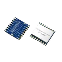
22 Uses0 StarsLORA-CC68-915MHz-TCXO
LORA-CC68-915MHz-TCXO is a compact, high-performance LoRa wireless transceiver module from NiceRF based on the Semtech LLCC68 chipset. Operating in the 915 MHz ISM band, it features a high-precision TCXO (Temperature-Compensated Crystal Oscillator) for improved frequency stability, making it ideal for long-range, low-power IoT and industrial wireless communication applications. The module supports LoRa, FSK, and GFSK modulation schemes, provides up to +22 dBm (160 mW) transmit power, and achieves receiver sensitivity as low as -129 dBm for extended communication range. It communicates through an SPI interface and is optimized for battery-powered and low-power systems. Key Features Based on Semtech LLCC68 LoRa transceiver chip 915 MHz ISM band operation High-precision TCXO for enhanced frequency stability Supports LoRa, FSK, and GFSK modulation Up to +22 dBm (160 mW) RF output power Receiver sensitivity up to -129 dBm SPI communication interface Operating voltage: 1.8 V to 3.7 V Low receive current (~6.5 mA typical) Integrated antenna switching circuitry Compact 16 mm × 16 mm SMD package Suitable for long-range and low-power wireless applications FCC-certified 915 MHz version RoHS compliant Typical Applications Smart Metering Industrial Automation Agricultural Monitoring Smart Cities Environmental Sensors Asset Tracking Warehouse Management Remote Control Systems Street Lighting Control Battery-Powered IoT Devices #CommonPartsLibrary #Module #LoRa #LLCC68 #915MHz #TCXO #WirelessModule #RFModule #IoT #IndustrialAutomation #SmartMetering #LongRangeCommunication #LowPowerDesign #SPI #EmbeddedSystems #NiceRF
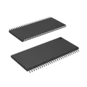
0 Uses0 StarsAS4C32M16SB-7TCN
SDRAM Memory IC 512Mbit Parallel 143 MHz 5.4 ns 54-TSOP II The AS4C32M16SB-7TCN is a single-data-rate synchronous dynamic random-access memory (SDR SDRAM) device manufactured by Alliance Memory. It is organized internally as a multi-bank array, allowing concurrent access operations across banks to improve effective memory bandwidth compared to simpler asynchronous DRAM architectures. The device is intended for general-purpose embedded memory applications where a synchronous, clock-driven memory interface is required, including embedded systems, industrial controllers, consumer electronics, networking equipment, and other designs that rely on a parallel SDRAM interface for working memory or buffering. As a drop-in style component within Alliance Memory's broader memory portfolio, this part is designed to be pin- and function-compatible with legacy SDR SDRAM devices originally offered by other manufacturers, allowing designers to source a continued-availability alternative for designs that depend on this memory architecture even as some original suppliers have discontinued production. This makes the device particularly useful in long-lifecycle industrial, embedded, and legacy system designs where a guaranteed supply of a specific memory interface and timing profile is critical to sustaining production over many years. The "B" designation in the part family indicates a specific die revision within the AS4C32M16S product line, reflecting a particular generation of internal silicon design while maintaining functional and pinout compatibility with related die revisions in the same footprint. The device communicates over a standard synchronous SDRAM command interface, using a clock-synchronized protocol for row and column addressing, data burst transfers, and bank management, and it supports the auto-refresh and self-refresh mechanisms typical of SDRAM devices to maintain stored data integrity without requiring constant external refresh management by the host controller. Mechanically, the device is housed in a thin small-outline package suited to space-constrained PCB layouts, and it is built for standard surface-mount assembly processes. The "-7TCN" suffix on this part number reflects a specific speed grade, package style, and temperature grade combination within the product family, with this particular variant intended for commercial temperature range operation. The device is supplied in tray packaging for surface-mount assembly and is compliant with RoHS material restrictions, supporting standard environmental and regulatory requirements for electronic components. Spec Sheet Identification Part Number: AS4C32M16SB-7TCN Device Family: AS4C32M16SB Manufacturer: Alliance Memory, Inc. Die Revision: B-die Functional Classification Device Type: Synchronous DRAM (SDR SDRAM) Memory Organization: Multi-bank array architecture Interface Type: Parallel, clock-synchronous command interface Refresh Capability: Supports auto-refresh and self-refresh modes Electrical Characteristics Supply Voltage: Standard 3.3V-class SDRAM supply rating Clock Frequency: Mid-range SDR SDRAM clock speed class Access Timing: Standard SDR SDRAM access time class for its speed grade Environmental & Qualification Temperature Grade: Commercial ("C" suffix designation) RoHS Compliance: Yes Product Positioning: Long-lifecycle, drop-in replacement memory device Package Package Type: Thin Small Outline Package, TSOP-II style Mounting: Surface mount technology (SMT) Packaging Format Supply Format: Tray packaging #AS4C32M16SB #AllianceMemory #SDRAM #SDRSDRAM #MemoryIC #EmbeddedMemory #TSOP #SurfaceMount #LegacyMemory #DropInReplacement #DRAM #EmbeddedSystems #IndustrialElectronics #SemiconductorIC #EngineeringSpec #ComponentLibrary #CommonPartsLibrary #RoHSCompliant #MemoryComponent #PCBDesign #CommonPartsLibrary #IntegratedCircuit #Memory #AS4C32
15 Uses0 StarsBM24-20DP/2-0.35V(51)
22 (20 + 2 Power) Position Connector Header, Outer Shroud Contacts Surface Mount Gold The BM24-20DP/2-0.35V(51) is a board-to-board and board-to-FPC header connector manufactured by Hirose Electric. It belongs to the BM24 series, a family of fine-pitch hybrid power and signal connectors designed for applications that require both data signaling and supplementary power delivery within the same compact interconnect, eliminating the need for a separate dedicated power connector alongside the signal interface. The connector functions as the plug (header) half of a mating pair, intended to mate with a corresponding BM24 receptacle to join two printed circuit boards, or a printed circuit board and a flexible printed circuit, in a low-profile board-to-board arrangement. This part number designates a configuration with a defined signal contact count supplemented by additional dedicated power contacts, reflecting the series' hybrid design philosophy in which the majority of positions handle signal or data lines while a smaller subset of positions is reserved for carrying higher current to support onboard power rails. This arrangement is particularly useful in compact consumer devices such as smartphones, wearables, and camera modules, where both data interfaces and local power distribution must be routed across a board-to-board junction without dedicating separate connectors to each function. The series is positioned by Hirose as supporting high-speed signaling standards including USB interfaces, making it suitable for applications that combine high-speed data transmission with power delivery in a single compact connector footprint. The connector's fine contact pitch and low mated height make it well suited to thin, space-constrained form factors where minimizing both footprint area and stack height is a priority. As with other Hirose board-to-board offerings, the connector is non-polarized in its base mechanical design, and it is supplied on embossed carrier tape for automated pick-and-place assembly, with construction compliant to RoHS material restrictions. Mechanically, the header is built to withstand the repeated mating cycles typical of consumer electronics manufacturing, rework, and field service, while maintaining stable, low-resistance contact across both its signal and power contact paths under realistic vibration and thermal conditions. As a header-style connector, it is intended to be soldered directly to a host PCB, with its mating receptacle counterpart soldered to the opposing board or FPC, allowing the assemblies to be joined and separated as needed throughout the product lifecycle. Spec Sheet Identification Part Number: BM24-20DP/2-0.35V(51) Series: BM24 Connector Style: Hybrid power/signal board-to-board and board-to-FPC connector Connector Type / Configuration Type: Header (plug) Gender: Male Orientation: Straight, surface mount Contact Arrangement: Hybrid configuration combining signal contacts and dedicated power contacts Polarization: Non-polarized Electrical Ratings Applicable High-Speed Protocols: USB2.0, USB3.0, USB3.1 (series capability) Transmission Rate: High-speed, multi-gigabit class (series capability) Power Contacts: Dedicated higher-current contacts integrated alongside signal contacts Mechanical Specifications Contact Pitch: Fine pitch Mounting Pitch: Matches contact pitch Mated Height: Low-profile Mounting Method: Surface mount technology (SMT) Mating Cycles: Rated for repeated mate/unmate cycles typical of consumer electronics assembly and rework Contact & Material Properties Contact Plating (Mating Area): Gold Insulator Material: High-temperature engineering resin suitable for SMT reflow Environmental Ratings RoHS Compliance: Yes Packaging Packaging Format: Embossed carrier tape, reel format Packaging Code Meaning: Suffix denotes embossed tape packaging at a standard reel quantity Mating Compatibility Mates With: Corresponding BM24 series receptacle connector Application Note: Intended for hybrid power and signal board-to-board or board-to-FPC interconnection in compact consumer electronics #BM24 #Hirose #HiroseElectric #BoardToBoard #BoardToFPC #HybridConnector #PowerAndSignal #Connector #SMTConnector #FinePitchConnector #USB #HighSpeedConnector #ConsumerElectronics #PCBDesign #HardwareEngineering #ConnectorDatasheet #EngineeringSpec #RoHSCompliant #ComponentLibrary #CommonPartsLibrary
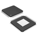
1 Uses0 StarsLAN9254-I/JRX
Ethernet Controller 10/100 Base-T/TX Bus Interface 80-TQFP-EP (12x12) The LAN9254-I/JRX is an EtherCAT SubDevice (slave) controller developed by Microchip Technology, designed to serve as the communication backbone for industrial automation devices participating in an EtherCAT network. The device integrates dual Ethernet physical layer transceivers directly on-chip, eliminating the need for external PHY components and simplifying the design of EtherCAT-enabled equipment such as servo drives, sensors, I/O modules, and other field devices used in real-time industrial control systems. Architecturally, the controller can operate as either a two-port or three-port node, depending on the network topology required. In its standard configuration it functions as a two-port device supporting daisy-chain connections typical of EtherCAT line topologies. When configured as a three-port device, it gains an additional management interface port that can connect to an external PHY or to another LAN9254, enabling star or tree network topologies and allowing the device to act as a branching point within a larger EtherCAT installation. Each integrated Ethernet PHY operates in full-duplex mode and supports automatic crossover detection, so the device can use either straight-through or crossover cabling without requiring manual configuration. Beyond pure protocol handling, the LAN9254 includes a substantial set of general-purpose digital input and output lines, allowing it to be used in simple field devices without requiring a separate microcontroller. For more complex applications, the device communicates with an external host processor through an integrated host bus interface that behaves like simple memory-mapped SRAM, supporting both 8-bit and 16-bit data widths along with multiple byte-ordering conventions, which makes it straightforward to interface with a wide range of microcontroller and microprocessor architectures. Internally, dual process data RAM buffers manage the exchange of real-time process data between the host application and the EtherCAT communication engine, while a dedicated interrupt line notifies the host of relevant internal events. A key feature of the device is its built-in distributed clock mechanism, which provides high-precision timing synchronization across all nodes in an EtherCAT network. This capability is essential for motion control and other applications where multiple devices must act in tight temporal coordination. The controller also provides configurable status indication through standard network activity and link LEDs, along with optional error and run-state indicators that give visibility into the health and operational state of the device at a glance. Power architecture on the LAN9254 is simplified through an integrated linear regulator, allowing the device to be operated from a single primary supply rail while internally generating the lower voltage needed for its core logic. This reduces the external power supply complexity that would otherwise be required to support separate core and I/O voltage domains. The "-I" designation on this particular part number indicates an industrial-grade temperature rating, making it suitable for deployment in factory floor and other demanding industrial environments where extended thermal range and long-term reliability are required. The device is housed in a surface-mount package consistent with dense industrial control board layouts and is compliant with RoHS material restrictions. Spec Sheet Identification Part Number: LAN9254-I/JRX Device Family: LAN9254 Manufacturer: Microchip Technology Functional Classification Device Type: EtherCAT SubDevice (slave) controller Network Role: Two/three-port configurable node Integrated PHYs: Dual Ethernet physical layer transceivers, on-chip Auto-MDIX Support: Yes, supports direct and crossover cabling Communication & Protocol Features Protocol: EtherCAT Topology Support: Daisy-chain (line), star, and tree topologies Additional Port Mode: Optional third port for branching/tap configurations Clock Synchronization: Integrated distributed clock for high-precision timing Host Interface Interface Type: SRAM-like host bus interface Data Width Support: Selectable bit-width host bus operation Endianness Support: Multiple byte-ordering modes Process Data Handling: Dual process data RAM buffers Interrupt Support: Configurable host interrupt line Digital I/O General-Purpose I/O: Integrated digital I/O lines for microcontroller-less operation Standalone Mode: Supports operation without external microcontroller for simple device designs Power Architecture Supply Configuration: Single primary supply rail Internal Regulation: Integrated linear regulator for core voltage generation Status Indication LED Support: Standard run and link/activity indicators per port Optional Indicators: Configurable error and run-state status indicators Environmental & Qualification Temperature Grade: Industrial ("-I" suffix) RoHS Compliance: Yes Package Package Type: Surface-mount, quad flat package style Mounting: Surface mount technology (SMT) Packaging Format Supply Format: Tape-and-reel, per part suffix designation #LAN9254 #Microchip #EtherCAT #SlaveController #SubDeviceController #IndustrialEthernet #IndustrialAutomation #MotionControl #EmbeddedSystems #FieldDevice #DigitalIO #HostBusInterface #DistributedClock #TQFP #RoHSCompliant #IndustrialGrade #EngineeringSpec #ComponentLibrary #CommonPartsLibrary #SemiconductorIC
1 Uses0 Stars150080M153000
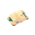
Red, Green, Blue (RGB) 624nm Red, 525nm Green, 470nm Blue LED Indication - Discrete 2V Red, 3.3V Green, 3.3V Blue 4-SMD, No Lead # 150080M153000 ## General Description The 150080M153000 is a compact surface-mount full-color RGB LED manufactured by Würth Elektronik as part of the WL-SFCD series. The device integrates red, green, and blue light-emitting elements within a single package, enabling the generation of a wide spectrum of colors for status indication, user interfaces, backlighting, visual notifications, and decorative lighting applications. Its diffused lens design provides uniform light distribution and wide viewing visibility, making it suitable for industrial equipment, consumer electronics, communication devices, instrumentation systems, control panels, and embedded electronic products. The component is optimized for automated assembly processes and offers reliable optical performance, low power consumption, and long operational life. ## Key Features ### Optical Characteristics * Full-color RGB light output * Integrated red, green, and blue emitters * Diffused lens design for uniform illumination * Wide viewing angle * High-visibility indication capability * Consistent color performance ### Electrical Characteristics * Low-power operation * Stable optical output * Suitable for indicator and backlighting applications * Reliable performance across operating conditions * Optimized for embedded electronic systems ### Mechanical Characteristics * Surface-mount package construction * Compact footprint * Low-profile package design * Compatible with automated assembly processes * Reflow-soldering compatible ### Package Construction * Common-anode configuration * Integrated multi-die LED architecture * Rectangular lens geometry * Lead-free package design * Industrial-grade construction ### Material Characteristics * High-quality encapsulation materials * Diffused optical lens * RoHS-compliant construction * Environmentally compliant materials ### Environmental Characteristics * Suitable for commercial and industrial applications * Long operational service life * Reliable operation under standard environmental conditions * Resistant to normal assembly and handling processes ### Application Areas * Status Indicators * User Interface Displays * Industrial Control Panels * Consumer Electronics * Home Appliances * Telecommunications Equipment * Instrumentation Systems * Backlighting Applications * Smart Devices * Embedded Electronic Products * Safety and Security Equipment * Human-Machine Interface Systems ### Compliance * RoHS Compliant * REACH Compliant * Lead-Free Compatible * Industry-Standard Surface-Mount Technology ## Manufacturer Würth Elektronik ## Product Family WL-SFCD SMD Full-Color Chip LED Series #150080M153000 #WurthElektronik #RGBLED #SMDLED #WLSFCD #FullColorLED #LEDIndicator #Backlighting #Optoelectronics #EmbeddedSystems #IndustrialElectronics #ConsumerElectronics #PCBDesign #ElectronicsEngineering #SMTAssembly #commonpartslibrary #optoelectronic #ledindication
332 Uses0 StarsSTM32MP157CAC3
ARM® Cortex®-A7 Microprocessor IC STM32MP1 2 Core, 32-Bit 209MHz, 650MHz 361-TFBGA (12x12) # Engineering Specification ## Product Name STM32MP157CAC3 ## General Description STM32MP157CAC3 is a high-performance microprocessor unit that combines application processing and real-time control capabilities within a single integrated circuit. The device is designed to support advanced embedded systems requiring a balance of computing performance, deterministic control, multimedia processing, connectivity, and security functionality. The component integrates multi-core processing resources, memory interfaces, graphics capabilities, peripheral controllers, and communication subsystems to enable the development of sophisticated embedded platforms. Its heterogeneous architecture allows high-level operating systems and real-time firmware to operate simultaneously, supporting applications that require both user-interface functionality and low-latency control. The device is intended for industrial automation, human-machine interface systems, edge computing platforms, communication equipment, medical devices, smart infrastructure, and Internet of Things applications. Its architecture enables consolidation of system functions, reducing component count and simplifying overall hardware design. The design emphasizes processing efficiency, system scalability, power management, security, and long-term reliability. It supports advanced software ecosystems and facilitates the development of connected embedded products with graphical interfaces, networking capabilities, and real-time operational control. ## Functional Requirements ### Application Processing The device shall provide application-level processing capabilities suitable for operating systems, middleware, and user applications. ### Real-Time Processing The device shall support deterministic control functions for time-critical embedded operations. ### Multimedia Support The component shall support graphical and multimedia processing functions for display and user-interface applications. ### System Integration The device shall integrate processing, communication, and peripheral functions within a unified embedded computing platform. ## Electrical Requirements ### Power Management The device shall support efficient power operation and multiple power management modes to optimize energy consumption. ### Memory Interface Support The component shall support external memory devices for program execution, data storage, and system operation. ### Peripheral Connectivity The device shall provide interfaces for communication, control, monitoring, and external subsystem integration. ### Signal Integrity The design shall support reliable operation across supported interface standards and operating conditions. ## Processing Architecture Requirements ### Multi-Core Operation The device shall support concurrent execution of application and real-time workloads through integrated processing resources. ### Operating System Support The architecture shall support embedded operating systems and software frameworks suitable for advanced application development. ### Security Features The device shall support hardware-based mechanisms intended to protect system integrity, software assets, and sensitive data. ### Resource Management The component shall support efficient allocation of processing, memory, and peripheral resources. ## Mechanical Requirements ### Surface Mount Construction The device shall be supplied in a high-density surface mount package suitable for automated manufacturing processes. ### PCB Integration The package shall support integration into multilayer printed circuit boards designed for high-performance embedded systems. ### Structural Integrity The device shall maintain electrical and mechanical reliability during assembly and operational service life. ## Environmental Requirements ### Operating Conditions The component shall operate reliably within environmental conditions commonly encountered in industrial and embedded applications. ### Thermal Performance The device shall support stable operation under sustained processing workloads and associated thermal conditions. ### Storage and Handling The component shall maintain physical and electrical integrity during transportation, storage, and manufacturing processes. ## Quality Requirements ### Reliability The device shall provide dependable long-term operation in embedded and industrial computing environments. ### Verification Processing, peripheral, communication, and system functions shall be validated through applicable testing and qualification procedures. ### Compliance The product shall conform to relevant semiconductor, quality, and embedded computing standards applicable to its intended use. ## Documentation Requirements Technical documentation shall include processor architecture information, hardware integration guidelines, memory interface recommendations, power management considerations, software development support, security features, and application design guidance. ## Classification Tags #STM32MP157CAC3 #STM32MP1 #Microprocessor #MPU #EmbeddedProcessor #ARMProcessor #EmbeddedLinux #RealTimeControl #IndustrialAutomation #HumanMachineInterface #EdgeComputing #IoTGateway #EmbeddedSystems #SystemOnChip #SoC #ApplicationProcessor #GraphicsProcessor #ConnectivityPlatform #IndustrialElectronics #PCBDesign #HardwareDevelopment #ElectricalEngineering #CommonPartsLibrary #ComponentLibrary #EngineeringSpecification #TechnicalDocumentation #SystemIntegration #SecureEmbeddedSystems #MulticoreProcessing
9 Uses0 Stars2286550-1
2286550-1 is a TE Connectivity Automotive HSD (High-Speed Data) hybrid connector header designed for high-speed data transmission in automotive applications. It is a shielded, right-angle PCB-mounted connector that combines HSD and MQS contacts, making it suitable for Ethernet, LVDS, USB, camera, infotainment, and other vehicle data communication systems. The connector features a 100 Ω controlled impedance design for reliable signal integrity in demanding automotive environments. Key Features Automotive HSD+2MQS hybrid header connector 6-position interface with A-coding Right-angle (horizontal) PCB mounting Board-to-board and wire-to-board connectivity Shielded construction for EMI protection 100 Ω impedance for high-speed data transmission Through-hole solder termination Operating voltage up to 60 VDC Maximum current rating: 2.5 A Operating frequency range: 0 to 3 GHz Gold-plated signal contacts for reliable performance Operating temperature range: -40°C to +105°C Reflow soldering capable Designed for automotive signal applications #CommonPartsLibrary #Connector #TEConnectivity #AutomotiveConnector #HSDConnector #DataConnectivity #HighSpeedData #AutomotiveEthernet #WireToBoard #BoardToBoard #ShieldedConnector #PCBConnector #AutomotiveElectronics #22865501
1 Uses0 Stars