Interface ICs
An interface IC is a type of integrated circuit that is designed to facilitate communication between two devices or systems. These devices are commonly used in electronic systems to enable the transfer of data and control signals between different components or subsystems. Some common use cases for interface ICs include connecting microcontrollers to peripherals such as sensors or displays, linking multiple processors together in a network, and enabling communication between devices using different communication protocols. Flux.ai has the world's largest community-driven public library of interface ICs, with footprints, symbols, datasheets, and simulation models. This library is a valuable resource for engineers and designers who need access to accurate and up-to-date information on these important components. Whether you are working on a new design project or simply looking to learn more about interface ICs, Flux.ai is an excellent resource to help you find the information you need.
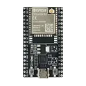
ESP32-DEVKITC-32UE
- ESP32-WROOM-32UE Transceiver; 802.11 b/g/n (Wi-Fi, WiFi, WLAN), Bluetooth® Smart Ready 4.x Dual Mode 2.4GHz Evaluation Board The ESP32-DEVKITC-32UE is a development board based on the ESP32 series SoC designed by Espressif. It is widely used for IoT, embedded systems, and wireless communication applications due to its built-in Wi-Fi and Bluetooth capabilities. Microcontroller: ESP32 dual-core Tensilica LX6 processor Wireless Connectivity: Wi-Fi (802.11 b/g/n) and Bluetooth (Classic + BLE) Flash Memory: Integrated SPI flash (varies by module version) Development Interface: USB-to-UART bridge for easy programming and debugging Power Supply: Typically powered via USB or external 5V input GPIO Pins: Multiple multifunction GPIOs supporting ADC, DAC, PWM, SPI, I2C, UART, etc. Supports deep sleep and ultra-low power modes Multiple peripheral interfaces (SPI, I2C, UART, SDMMC, PWM) Compatible with ESP-IDF, Arduino IDE, and MicroPython Built-in antenna (UE variant uses U.FL or external antenna option depending on module design) IoT devices and smart home systems Wireless sensor networks Data logging and monitoring systems Robotics and automation Embedded control systems #commonpartslibrary #developmentboard #esp32 #wroom
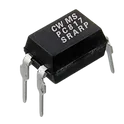
1.0k Uses7 StarsPC817C-S
SOP-4-2.54mm Transistor, Photovoltaic Output Optoisolators ROHS PC817C-S SOP-4_L6.5-W4.6-P2.54-LS10.3-TL LCSC Part Number: C3008369 JLCPCB Part Class: Extended Part Manufactured by UMW(友台半导体) The ESDA18-1K is a transient voltage suppression and electrostatic discharge protection device designed to protect sensitive electronic circuits from ESD events, surge transients, and electrical overstress conditions. Manufactured by STMicroelectronics and commonly used in communication and embedded electronic systems, this device provides fast-response protection for signal lines and low-voltage interfaces exposed to external electrical disturbances. The component utilizes low-capacitance TVS diode technology to clamp transient voltages while maintaining signal integrity on high-speed communication lines. It is optimized for protecting USB interfaces, GPIO lines, communication ports, sensor interfaces, and portable electronic devices from electrostatic discharge damage and transient spikes. The ESDA18-1K is widely used in industrial electronics, consumer devices, embedded systems, communication hardware, and portable equipment requiring compact and reliable ESD suppression. Its small surface-mount package enables easy integration into high-density PCB layouts while improving overall system reliability and EMC robustness. Engineering Specification Device Type Transient voltage suppression and ESD protection diode Protection Function Electrostatic discharge and surge transient suppression Protection Architecture Single-line TVS protection structure Response Characteristics Fast transient clamping response Signal Compatibility Suitable for low-voltage and high-speed signal interfaces Capacitance Characteristics Low capacitance for minimal signal distortion Electrical Performance Low leakage current and stable clamping behavior Reliability Features High ESD robustness and transient tolerance Mounting Style Surface mount technology Package Type Compact SOD-style surface-mount package Thermal Characteristics Low-power passive protection structure EMC Features Enhanced electromagnetic compatibility protection support Applications USB interface protection GPIO protection Communication interfaces Embedded systems Portable electronics Industrial control hardware Sensor interfaces Consumer electronics Signal line protection Data communication systems Manufacturer STMicroelectronics #commonpartslibrary #esdprotection #tvsdiode #transientprotection #signalprotection #stmicroelectronics #embeddedhardware #electronicsdesign
349 Uses2 StarsMAX98357AETE+T
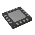
MAX98357A Series 5.5V 3.2W PCM Input Class D Audio Power Amplifier - TQFN-16 The MAX98357A/MAX98357B is an easy-to-use, low-cost, digital pulse-code modulation (PCM) input Class D amplifier that provides industry-leading Class AB audio performance with Class D efficiency. The digital audio interface automatically recognizes up to 35 different PCM and TDM clocking schemes which eliminates the need for I2C programming. Operation is further simplified by eliminating the need for an external MCLK signal that is typically used for PCM communication. Simply supply power, LRCLK, BCLK, and digital audio to generate audio! Furthermore, a novel pinout allows customers to use the cost-effective WLP package with no need for expensive vias (refer to Application Note 6643: Optimize Cost, Size, and Performance with MAX98357 WLP for more information). The digital audio interface is highly flexible with the MAX98357A supporting I2S data and the MAX98357B supporting left-justified data. Both ICs support 8 channel time division multiplexed (TDM) data. The digital audio interface accepts specified sample rates between 8kHz and 96kHz for all supported data formats. The ICs can be configured to produce a left channel, right channel, or (left/2 + right/2) output from the stereo input data. The ICs operate using 16/24/32-bit data for I2S and left-justified modes as well as 16-bit or 32-bit data using TDM mode. The ICs eliminate the need for the external MCLK signal that is typically used for PCM communication. This reduces EMI and possible board coupling issues in addition to reducing the size and pin count of the ICs. The ICs also feature a very high wideband jitter tolerance (12ns typ) on BCLK and LRCLK to provide robust operation. Active emissions-limiting, edge-rate limiting, and overshoot control circuitry greatly reduce EMI. A filterless spread-spectrum modulation scheme eliminates the need for output filtering found in traditional Class D devices and reduces the component count of the solution. The ICs are available in 9-pin WLP (1.345mm x 1.435mm x 0.64mm) and 16-pin TQFN (3mm x 3mm x 0.75mm) packages and are specified over the -40°C to +85°C temperature range. ● Single-Supply Operation (2.5V to 5.5V) ● 3.2W Output Power into 4Ω at 5V ● 2.4mA Quiescent Current ● 92% Efficiency (RL = 8Ω, POUT = 1W) ● 22.8μVRMS Output Noise (AV = 15dB) ● Low 0.013% THD+N at 1kHz ● No MCLK Required ● Sample Rates of 8kHz to 96kHz ● Supports Left, Right, or (Left/2 + Right/2) Output ● Sophisticated Edge Rate Control Enables Filterless Class D Outputs ● 77dB PSRR at 1kHz ● Low RF Susceptibility Rejects TDMA Noise from GSM Radios ● Extensive Click-and-Pop Reduction Circuitry ● Robust Short-Circuit and Thermal Protection ● Available in Space-Saving Packages: 1.345mm x 1.435mm WLP (0.4mm Pitch) and 3mm x 3mm TQFN ● Solution Size with Single Bypass Capacitor is 4.32mm2 Applications ● Single Li-ion Cell/5V Devices ● Smart Speakers ● Notebook Computers ● IoT Devices ● Gaming Devices (Audio and Haptics) ● Smartphones ● Tablets ● Cameras #commonpartslibrary #integratedcircuit #linearamplifier #mono
1.2k Uses2 StarsADXL345BCCZ-RL
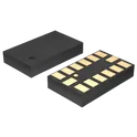
Accelerometer X, Y, Z Axis ±2g, 4g, 8g, 16g 0.05Hz ~ 1.6kHz 14-LGA (3x5) The ADXL345 is a small, thin, ultralow power, 3-axis accelerometer with high resolution (13-bit) measurement at up to ±16 g. Digital output data is formatted as 16-bit twos complement and is accessible through either a SPI (3- or 4-wire) or I2C digital interface. The ADXL345 is well suited for mobile device applications. It measures the static acceleration of gravity in tilt-sensing applications, as well as dynamic acceleration resulting from motion or shock. Its high resolution (3.9 mg/LSB) enables measurement of inclination changes less than 1.0°. Several special sensing functions are provided. Activity and inactivity sensing detect the presence or lack of motion by comparing the acceleration on any axis with user-set thresholds. Tap sensing detects single and double taps in any direction. Free-fall sensing detects if the device is falling. These functions can be mapped individually to either of two interrupt output pins. An integrated memory management system with a 32-level first in, first out (FIFO) buffer can be used to store data to minimize host processor activity and lower overall system power consumption. Low power modes enable intelligent motion-based power management with threshold sensing and active acceleration measurement at extremely low power dissipation. The ADXL345 is supplied in a small, thin, 3 mm × 5 mm × 1 mm, 14-lead, plastic package. ► Ultralow power: as low as 23 µA in measurement mode and 0.1 µA in standby mode at VS = 2.5 V (typical) ► Power consumption scales automatically with bandwidth ► User-selectable resolution ► Fixed 10-bit resolution ► Full resolution, where resolution increases with g range, up to 13-bit resolution at ±16 g (maintaining 4 mg/LSB scale factor in all g ranges) ► Embedded memory management system with FIFO technology minimizes host processor load ► Single tap/double tap detection ► Activity/inactivity monitoring ► Free-fall detection ► Supply voltage range: 2.0 V to 3.6 V ► I/O voltage range: 1.7 V to VS ► SPI (3- and 4-wire) and I2C digital interfaces ► Flexible interrupt modes mappable to either interrupt pin ► Measurement ranges selectable via serial command ► Bandwidth selectable via serial command ► Wide temperature range (−40°C to +85°C) ► 10,000 g shock survival ► Pb free/RoHS compliant #commonpartslibrary #sensor #transducer #accelerometer
203 Uses2 StarsMMBT3904-TP
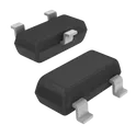
Bipolar (BJT) Transistor NPN 40V 200mA 300MHz 350mW Surface Mount SOT-23 The MMBT3904-TP is an NPN general-purpose bipolar junction transistor (BJT) in a SOT-23 surface-mount package. It is a compact SMD version of the classic 2N3904, designed for switching and low-power signal amplification in a wide range of electronic circuits. It is commonly used in embedded systems, consumer electronics, and PCB designs where small size and reliable switching performance are required. Key Features NPN Bipolar Junction Transistor (BJT) Suitable for switching and amplification applications SOT-23 Surface-Mount Package Compact footprint for high-density PCB designs Collector-Emitter Voltage (Vceo) Typically up to 40V Collector Current Up to 200 mA continuous Low Power Operation Designed for small signal and low-power switching tasks High Gain (hFE) DC current gain typically 100–300 Fast Switching Capability Suitable for digital and pulse applications Wide Operating Temperature Range Typically -55°C to +150°C High Reliability Stable performance for general-purpose use RoHS Compliant Environmentally compliant manufacturing Typical Applications Signal switching in digital circuits LED driving circuits Small relay or load switching Sensor interface circuits General-purpose amplification stages 2N3904 SOT-23 #CommonPartsLibrary #Transistor #BJT #NPN #MMBT3904
732 Uses2 StarsPIC16F877A-I/P
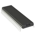
PIC PIC® 16F Microcontroller IC 8-Bit 20MHz 14KB (8K x 14) FLASH 40-PDIP The PIC16F877A-I/P is a high-performance 8-bit microcontroller from Microchip Technology, based on a Harvard architecture with separate program and data memory buses. It is designed for a wide range of embedded applications requiring reliable processing, multiple communication interfaces, and analog capability. The device integrates Flash program memory, EEPROM data storage, and numerous peripherals including ADC, timers, serial communication modules, and PWM functions. Packaged in a 40-pin PDIP form factor, it is widely used in industrial automation, consumer electronics, and educational development systems. Core Features 8-bit PIC microcontroller architecture Harvard architecture with RISC instruction set Operating frequency up to 20 MHz Single-cycle instruction execution (except branches) Memory Program Memory: 8K words (Flash) Data Memory (RAM): 368 bytes EEPROM Data Memory: 256 bytes I/O Features Up to 33 programmable I/O pins Multiple input/output ports (PORTA, PORTB, PORTC, PORTD, PORTE) High current sink/source capability on selected pins Analog Features 10-bit Analog-to-Digital Converter (ADC) Up to 8 analog input channels Programmable voltage reference Timers and Control Three timers (Timer0, Timer1, Timer2) Capture/Compare/PWM (CCP) modules Watchdog Timer (WDT) Power-on Reset (POR) and Brown-out Reset (BOR) Communication Interfaces USART (Universal Synchronous/Asynchronous Receiver/Transmitter) SPI (Serial Peripheral Interface) I²C (Inter-Integrated Circuit) via MSSP module Electrical Characteristics Operating Voltage: 4.0V to 5.5V Operating Temperature Range: -40°C to +85°C (Industrial grade) Low power consumption modes available Package Information Package Type: PDIP (Plastic Dual Inline Package) Pin Count: 40 pins Mounting Type: Through-hole Applications Industrial control systems Embedded automation Consumer electronics Sensor interfacing and data acquisition Educational and prototyping platforms #commonpartslibrary #integratedcircuit #microcontroller
873 Uses2 Stars
Page 1 of 46
Next