Capacitors
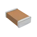
A capacitor is a passive electronic component that stores electrical charge and is commonly used to store energy in a circuit. Capacitors are used in a wide range of applications including power supply filtering, signal coupling, and decoupling, noise suppression, and voltage dividing. One of the main use cases of capacitors is to smooth out fluctuations in a direct current (DC) power supply by acting as a temporary reservoir of electrical charge. Capacitors can also be used to block the flow of direct current while allowing alternating current to pass, making them useful for signal coupling and decoupling in audio and radio frequency circuits. Flux.ai is the world's largest community-driven public library of capacitors, offering footprints, symbols, datasheets, and simulation models for a wide range of capacitor types. Whether you're an engineer looking for detailed technical information or a maker in need of resources for your latest project, Flux.ai has you covered.
FT0H474ZF
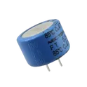
470 mF (EDLC) Supercapacitor 5.5 V Radial, Can 6.5Ohm @ 1kHz The FT0H474ZF is a 5.5 V electric double-layer capacitor (EDLC), also known as a supercapacitor, manufactured by KEMET. It provides 470 mF (0.47 F) of capacitance for energy storage, backup power, and short-duration power hold-up applications. Designed for through-hole mounting in a radial can package, it offers high reliability, a wide operating temperature range, and long cycle life, making it suitable for memory backup, RTC backup, industrial electronics, and low-power energy storage systems. Key Features 470 mF (0.47 F) capacitance 5.5 V rated voltage Electric Double-Layer Capacitor (EDLC) technology Radial through-hole package Long operational life with excellent charge/discharge cycle capability Wide operating temperature range: −40°C to +85°C Low maintenance energy storage solution Suitable for backup power, memory retention, and peak power assistance RoHS compliant Reliable performance for industrial and consumer electronic applications #KEMET #Supercapacitor #EDLC #EnergyStorage #BackupPower #MemoryBackup #PowerHoldUp #RadialCapacitor #ThroughHole #Electronics #IndustrialElectronics #LowPowerDesign #CommonPartsLibrary #Capacitor
0 Uses0 Stars476BPS050M
47µF 50V Aluminum Electrolytic Capacitors Radial, Can 5.644Ohm @ 120Hz 2000 Hrs @ 85°C The 476BPS050M is a 47 µF, 50 V non-polar (bi-polar) aluminum electrolytic capacitor from the BPS series of Cornell Dubilier. It is a radial lead through-hole capacitor designed for AC signal coupling and crossover network applications where polarity cannot be guaranteed. The capacitor offers reliable performance with a long operational life and compact package size. Capacitance: 47 µF Rated Voltage: 50 VDC Non-polar / Bi-polar construction Radial leaded through-hole package Operating temperature range: -40°C to +85°C Load life: 2,000 hours at 85°C Suitable for audio coupling and crossover networks Compact aluminum electrolytic design RoHS-compliant lead-free construction (series dependent) Typical Applications Audio coupling circuits Speaker crossover networks AC signal filtering General-purpose non-polar capacitor applications Analog signal processing circuits #CornellDubilier #BPSSeries #ElectrolyticCapacitor #BiPolarCapacitor #47uF #50V #ThroughHole #AudioElectronics #CrossoverNetwork #PassiveComponents #ElectronicDesign #CommonPartsLibrary #Capacitor #SMD #polarize
0 Uses0 StarsTPS259540DSGT
All details fully confirmed from Texas Instruments' official datasheet, DigiKey, and multiple verified distributor sources. Here's the complete spec. Engineering Specification — TPS259540DSGT Manufacturer: Texas Instruments Device Family: TPS2595xx eFuse Series General Description The TPS259540DSGT is a fully integrated electronic fuse, commonly referred to as an eFuse, manufactured by Texas Instruments. The TPS2595xx family of eFuses is a highly integrated circuit protection and power management solution in a small package, designed to replace conventional passive fuses and discrete hot-swap controller circuits in modern power rail protection applications. Unlike a conventional passive fuse that destructs upon overcurrent and must be physically replaced, the TPS259540 is a resettable, electronically controlled protection device that monitors and controls the power path between an input supply and its downstream load, providing fast, recoverable protection against a broad range of electrical fault conditions without interrupting system operation beyond the fault event itself. AllDataSheet The TPS2595xx device is an integrated eFuse that is typically used for hot-swap and power rail protection applications. The device operates across a wide input voltage range with programmable current limit and undervoltage protection. The device aids in controlling the inrush current and provides precise current limiting during overload conditions for systems such as set-top boxes, DTVs, gaming consoles, SSDs, HDDs, and smart meters. The device also provides robust protection for multiple faults on the sub-system rail. Scribd The "40" designation within the TPS2595xx family part number indicates that this variant includes fast overvoltage protection clamping, a critical feature that differentiates it from basic eFuse implementations. Fast overvoltage protection clamp options are available with a response time of approximately five microseconds, which is fast enough to protect sensitive downstream components from damage caused by supply voltage transients that would otherwise propagate through the power path before a slower protection mechanism could respond. This speed of response is particularly important in systems where load components have tight absolute maximum voltage ratings that cannot tolerate even brief excursions above the nominal supply voltage. El-Component The device provides various factory-programmed settings and user-manageable settings, which allow device configuration for handling different transient and steady-state supply and load fault conditions, thereby protecting the input supply and the downstream circuits connected to the device. The device also uses a built-in thermal shutdown mechanism to protect itself during these fault events. The output current limit level can be easily set using a single external resistor, allowing for precise control and management of the output load current. Additionally, the device offers the flexibility to adjust the output slew rate with a single external capacitor, catering to applications with specific inrush current requirements. ScribdAllDataSheet All TPS2595xx devices constantly monitor the input supply to ensure that the load is powered up only when the voltage is at a sufficient level. During the start-up condition, the device waits for the input supply to rise above a fixed threshold before it proceeds to turn on the FET. Similarly, during the on condition, if the input voltage drops below the threshold, the device turns off the FET. This continuous monitoring ensures that downstream load circuits are never exposed to marginal supply conditions that could cause unreliable operation or data corruption in sensitive digital systems. Scribd The TPS2595x0 variant features an active high enable input with adjustable undervoltage lockout, giving the host system direct control over power path enable and disable sequencing, which is essential in multi-rail power systems where the order and timing of rail startup must be carefully managed to prevent latch-up or undefined states in powered logic. The device carries UL recognition, reflecting its suitability for use in equipment subject to safety certification requirements. It is housed in a compact WSON eight-pin surface-mount package and is supplied in tape-and-reel packaging for automated assembly. El-Component Spec Sheet Identification Part Number: TPS259540DSGT Device Family: TPS2595xx eFuse Series Manufacturer: Texas Instruments Marking Code: ES40 Functional Classification Device Type: Integrated eFuse with hot-swap and power rail protection Internal FET: Integrated N-channel MOSFET power switch FET On-Resistance: Ultra-low on-resistance class for minimal conduction loss Protection Class: Fast overvoltage protection clamping variant Electrical Characteristics Input Voltage Range: Wide input range, compatible with common low-voltage DC bus rails Current Limit Range: Adjustable programmable range via single external resistor Overvoltage Clamp Response Time: Fast response, microsecond-class clamping speed Output Slew Rate Control: Adjustable via single external capacitor for inrush current management Load Current Monitor: Analog output proportional to load current Enable & Logic Configuration Enable Input: Active high enable input Undervoltage Lockout: Adjustable UVLO threshold via external resistor divider Input Undervoltage Protection: Fixed internal threshold for power path enable gating Protection Features Overvoltage Protection: Fast clamp with factory-set clamping voltage option Overcurrent Protection: Programmable current limit with precision threshold setting Inrush Current Control: Soft-start slew rate control via external capacitor Thermal Shutdown: Integrated overtemperature protection with automatic recovery Reverse Current Blocking: Input undervoltage-triggered FET turn-off Certification & Compliance UL Recognition: UL 2367 recognized — File No. E169910 Export Classification: EAR99 RoHS Compliance: Yes Target Applications Hot-swap power path management Power rail protection for set-top boxes, gaming consoles, and smart meters SSD and HDD power management Digital TV and consumer AV subsystem power protection Industrial multi-rail power sequencing IoT and embedded system power protection Package Package Type: WSON — Small Outline No-Lead, eight-pin Package Designation: DSG suffix Mounting Method: Surface mount technology (SMT) Packaging Format Supply Format: Tape-and-reel — DSGT suffix #TPS259540 #TPS2595xx #TexasInstruments #eFuse #HotSwap #PowerRailProtection #OvervoltageProtection #CurrentLimit #InrushControl #PowerManagement #WSON #SurfaceMount #IntegratedFET #CircuitProtection #PowerSequencing #SmartPower #SemiconductorIC #EngineeringSpec #ComponentLibrary #CommonPartsLibrary #RoHSCompliant #ULRecognized
10 Uses0 StarsDRV8770RGER
Half Bridge (2) Driver DC Motors, General Purpose NMOS, Power MOSFET 24-VQFN (4x4) The DRV8770RGER is a high-voltage brushed DC motor gate driver integrated circuit manufactured by Texas Instruments, designed to drive external N-channel power MOSFETs configured in a dual half-bridge topology for use in brushed DC motor control, stepper motor drive, solenoid actuation, and other inductive load switching applications. Rather than integrating the power stage transistors directly within the IC, the DRV8770 functions as a gate driver, providing the gate voltage and current needed to fully and rapidly switch external discrete power MOSFETs, which allows the designer to choose power devices appropriate to the specific voltage and current requirements of their motor or load without being constrained by the internal power stage of an integrated motor driver. The DRV8770 delivers two half-bridge gate drivers, each capable of driving high-side and low-side N-channel power MOSFETs. The integrated bootstrap diode and external capacitor generate the correct gate drive voltages for the high-side MOSFETs, while the GVDD rail drives the gates of the low-side MOSFETs. This bootstrap architecture eliminates the need for an external isolated gate drive power supply for the high-side switch, simplifying the overall power stage design significantly compared to approaches that require separate high-side power supply generation. This device decreases system component count, reduces PCB area, and saves cost by integrating two independent half-bridge gate drivers and bootstrap diodes. digikeyTME The high-side and low-side gate drivers can drive source and sink currents sufficient for fast, efficient switching of external power MOSFETs, with total average output current capability defined in the datasheet. The asymmetric source and sink current capability is a deliberate design choice reflecting the typical requirements of power MOSFET switching, where rapid turn-off is often more critical than turn-on speed for preventing shoot-through and managing switching losses in bridge circuits. Small propagation delay and delay matching specifications minimize the dead-time requirement, which further improves efficiency. TMEFarnell The high voltage tolerance of the gate drive pins improves system robustness. The SHx phase pins can tolerate significant negative voltage transients, while the high-side gate driver supply can support higher positive voltage transients on the BSTx and GHx pins. This enhanced transient tolerance is essential in motor drive applications where inductive switching generates voltage spikes and negative voltage excursions on the switch node that would damage less robust gate driver designs. An input deglitcher prevents high-frequency noise on the input pins from affecting the output state of the gate drivers, protecting against inadvertent switching caused by electrical noise on the control interface lines. FarnellAllDataSheet The device can drive one or two DC brush motors, one stepper motor, solenoids, or other inductive loads. This versatility makes it suitable across a broad range of actuator types within the same hardware platform, allowing a single PCB design to serve multiple product variants by simply changing the connected load and the firmware control scheme. Undervoltage protection is provided for both low-side and high-side through GVDD and BST undervoltage lockout, preventing the external power MOSFETs from operating with insufficient gate drive voltage, which would cause them to enter a linear operating region with excessive power dissipation and potential thermal damage. digikeyFarnell The DRV8770RGER is housed in a compact VQFN twenty-four-pin surface-mount package, suited to space-constrained motor drive PCB layouts, and is rated for operation across an extended industrial temperature range. Spec Sheet Identification Part Number: DRV8770RGER Device Family: DRV8770 Manufacturer: Texas Instruments Functional Classification Device Type: Dual half-bridge N-channel MOSFET gate driver IC Topology: Two independent half-bridge gate drivers Application Class: Brushed DC motor, stepper motor, solenoid, and inductive load drive Gate Drive Architecture High-Side Driver: Bootstrap-based gate drive with integrated bootstrap diode Low-Side Driver: GVDD-referenced direct gate drive Gate Drive Current — Source: High source current capability for rapid MOSFET turn-on Gate Drive Current — Sink: Higher sink current capability for rapid MOSFET turn-off Voltage Ratings Maximum Operating Voltage: High-voltage class, suited to industrial motor supply rails Phase Pin Transient Tolerance: Rated for negative voltage transients on SHx switch node pins Bootstrap Pin Transient Tolerance: Elevated absolute maximum on BSTx and GHx pins for spike immunity Timing & Switching Performance Propagation Delay: Small and tightly specified for minimal dead-time requirement Delay Matching: High-side to low-side delay matching for improved bridge efficiency Input Deglitching: Built-in input deglitch filter to suppress high-frequency noise on control inputs Protection Features GVDD Undervoltage Lockout: Protects low-side gate drive from insufficient supply BST Undervoltage Lockout: Protects high-side gate drive from insufficient bootstrap voltage Negative Transient Tolerance: Phase pins rated for switch-node negative voltage excursions Load Compatibility Supported Load Types: Brushed DC motors, stepper motors, solenoids, and general inductive loads Drive Configurations: Single or dual brushed DC motor, single stepper motor, or independent half-bridge loads Environmental & Qualification Operating Temperature Range: Extended industrial temperature range RoHS Compliance: Yes Lifecycle Status: Active production Package Package Type: VQFN — Very thin Quad Flat No-Lead, twenty-four-pin Package Suffix: RGER designation Mounting Method: Surface mount technology (SMT) Package Pitch: Fine pitch, compact footprint Packaging Format Supply Format: Tape-and-reel, cut-tape, and custom reel options available #DRV8770 #DRV8770RGER #TexasInstruments #GateDriver #HalfBridgeDriver #BrushedDCMotor #MotorDriver #StepperMotorDriver #SolenoidDriver #NChannelMOSFET #BootstrapDriver #HighVoltageDriver #PowerElectronics #MotorControl #InductiveLoad #VQFN #SurfaceMount #SemiconductorIC #EngineeringSpec #ComponentLibrary #CommonPartsLibrary #RoHSCompliant #IndustrialMotorDrive
1 Uses0 StarsIQS7222B102QNR
All details fully confirmed from Azoteq's official IQS7222B datasheet and multiple verified distributor sources. Here's the complete spec. Engineering Specification — IQS7222B102QNR Manufacturer: Azoteq (Pty) Ltd Device Family: IQ Switch® ProxFusion® Series — IQS7222B General Description The IQS7222B102QNR is a high-channel-count capacitive touch and proximity sensing controller integrated circuit manufactured by Azoteq, belonging to the ProxFusion series of intelligent human interface sensing devices. The IQS7222B is a sensor fusion device for various multi-button applications that is fully I²C compatible, with on-chip calculations that enable the IC to respond effectively even in the lowest-power modes. It represents an expanded-channel evolution within Azoteq's IQS7222 family, offering a substantially higher mutual capacitance channel count than the IQS7222A variant while maintaining the same ProxFusion design philosophy of combining sophisticated on-chip sensing intelligence with a minimal external component requirement and a compact surface-mount package. Molex The IQS7222B is a highly flexible ProxFusion device that can configure up to eighteen mutual capacitance buttons or up to eight self-capacitance buttons, with nine external sensor pad connections available in the QFN package variant. Alternatively, it can configure up to twenty mutual capacitance buttons or eighteen mutual capacitance buttons with a proximity wake-up function. This high degree of channel configurability makes the device adaptable to a very broad range of physical interface configurations, from simple multi-button panels to complex touch arrays with simultaneous proximity wake-up capability, all within a single fixed-footprint IC that does not require a change of device between product variants with different button counts. MolexAmazon Target applications for the IQS7222B include remote control user interfaces, home automation device user interfaces, and wireless speaker controls. These application domains share common requirements for robust touch detection through cosmetic overlay materials such as glass, plastic, or painted surfaces, reliable operation in environments where the device may be exposed to moisture or contamination, and power efficiency sufficient to support battery-powered or always-on operation without significantly impacting battery life. The device's on-chip power management architecture, which features automated system power modes for optimal response versus consumption, directly addresses these requirements by allowing the device to spend the majority of its time in a low-current sleep or ultra-low-power state while still waking promptly in response to proximity or touch events. MolexMolex Built-in basic functions include automatic tuning, noise filtering, debounce and hysteresis, and dual direction trigger indication. The automatic tuning capability, implemented through Azoteq's proprietary ATI algorithm, compensates for variations in electrode capacitance that arise from PCB manufacturing tolerances, overlay thickness variation, and environmental factors such as temperature and supply voltage drift. This self-calibration eliminates the need for individual unit factory calibration and ensures consistent touch sensitivity across the full production run of any product built around this device. The noise filtering and debounce functions further improve the reliability of touch event detection in electrically noisy environments, preventing false triggers from electrical interference or mechanical vibration that could otherwise cause spurious button events in poorly filtered designs. Molex Both mutual capacitance and self-capacitance designs are possible with the IQS7222B, giving system designers the flexibility to choose the sensing modality most appropriate for their electrode layout and overlay configuration. Mutual capacitance sensing offers better noise immunity and the ability to detect touch through thicker overlay materials, while self-capacitance sensing allows a simpler single-electrode layout per button with potentially higher raw sensitivity. The I²C communication interface supports IRQ/RDY signaling at speeds up to Fast-Plus mode, providing efficient, low-latency event notification to the host microcontroller without requiring continuous polling of the device. The "QNR" suffix in the part number designates the QFN twenty-pin package variant, which offers the maximum external pad count for mutual capacitance configurations. MolexMolex Spec Sheet Identification Part Number: IQS7222B102QNR Device Family: IQ Switch ProxFusion Series — IQS7222B Manufacturer: Azoteq (Pty) Ltd Part Number Decode IQS7222B: Base device family, B-variant expanded channel count 102: Firmware/configuration variant designation QNR: QFN twenty-pin package, tape-and-reel Functional Classification Device Type: Multi-channel capacitive touch and proximity sensing controller IC Sensing Architecture: ProxFusion sensor fusion engine with on-chip processing Application Class: Multi-button, slider, and wheel human interface controller Channel Configuration Mutual Capacitance Buttons: Up to twenty configurable buttons Mutual Capacitance with Proximity Wake-Up: Up to eighteen mutual capacitance buttons with simultaneous proximity wake function Self-Capacitance Buttons: Up to eight self-capacitance buttons External Sensor Pad Connections: Nine pads available in QFN package Sensing Modalities Mutual Capacitance: Full channel array for high noise immunity and overlay penetration Self-Capacitance: Simplified single-electrode per button layout option Proximity Detection: Pre-touch proximity wake-up capability Built-In Processing Functions Automatic Tuning: Proprietary ATI algorithm for self-calibration and baseline normalization Noise Filtering: Integrated digital filtering for EMI and environmental noise rejection Debounce and Hysteresis: Per-channel configurable debounce and release hysteresis Dual Direction Trigger: Positive and negative delta event detection Host Interface Communication Protocol: I²C fully compatible Speed Grade: Up to Fast-Plus mode Event Signaling: IRQ/RDY interrupt output for host notification I²C Address: Configurable; additional address options available on special request Power Management Operating Modes: Active sensing, idle, and ultra-low-power modes Automated Power Mode Control: System-managed transitions for optimized response versus current consumption ULP Wake Capability: Proximity or touch event wake-up from ultra-low-power state Layout & Application Notes VREG Decoupling: Capacitor required at each VREG pin, placed as close as possible to IC Tx Series Resistance: Nominal series resistance recommended on Rx electrodes to reduce EMI coupling ESD Rating: Pins rated to high HBM ESD performance per JEDEC JEP155 Environmental & Qualification RoHS Compliance: Yes Lifecycle Status: Active production Package Package Type: QFN — Quad Flat No-Lead, twenty-pin Package Designation: QNR variant per Azoteq ordering suffix Mounting Method: Surface mount technology (SMT) Packaging Format Supply Format: Tape-and-reel Target Applications Remote control user interfaces Home automation device controls Wireless speaker and audio device interfaces Multi-button consumer appliance panels IoT device touch interfaces Industrial HMI panels with overlay #IQS7222B #IQS7222B102QNR #Azoteq #ProxFusion #IQSwitch #CapacitiveTouchController #MutualCapacitance #SelfCapacitance #ProximityController #MultiButtonHMI #TouchSensor #ATICalibration #SmartHMI #HomeAutomation #RemoteControl #WirelessSpeaker #IoTDesign #LowPowerSensing #QFN20 #SurfaceMount #EmbeddedHMI #EngineeringSpec #ComponentLibrary #CommonPartsLibrary #RoHSCompliant
2 Uses0 StarsXL1509-5.0E1
2A 150KHz 40V Buck DC to DC Converter The XL1509-5.0E1 is a fixed frequency PWM buck step-down DC-DC converter capable of driving a load with high efficiency, low ripple, and excellent line and load regulation. It is manufactured by XLSEMI and belongs to the XL1509 product family, a series of fixed-output and adjustable-output step-down switching regulator ICs designed to simplify the design of compact, efficient DC power conversion stages in a wide range of embedded, industrial, and consumer electronics applications. The "5.0" designation in the part number specifies that this variant produces a fixed regulated output voltage of five volts, making it directly suited to powering five-volt logic, microcontrollers, sensors, communication modules, and other standard digital subsystems from higher-voltage DC rails without requiring a linear regulator and its inherent power dissipation penalty. Unikeyic Electronics The XL1509 requires a minimum number of external components, making it simple to use, and includes internal frequency compensation and a fixed-frequency oscillator. The PWM control circuit is able to adjust the duty ratio linearly from zero to one hundred percent. This internal compensation architecture removes the burden of control loop design from the system engineer, which is a common point of complexity in discrete buck converter designs, and allows the device to be implemented with a straightforward application circuit consisting of an input capacitor, an output inductor, a freewheeling Schottky diode, and an output capacitor, without requiring additional feedback network components in the fixed-output version. Unikeyic Electronics The device operates across a wide input voltage range, accepting input rails ranging from just above the output voltage all the way up to the high end of the input range, making it compatible with a variety of common source voltages including twelve-volt, twenty-four-volt, and other industrial bus rails frequently encountered in embedded and industrial power system designs. This wide input range also makes it suitable for battery-powered applications where the supply voltage varies considerably across the battery discharge cycle, as the converter maintains a regulated output throughout the input voltage window. The fixed switching frequency is set internally at a value that represents a practical tradeoff between external component size and switching loss, allowing the use of standard commodity inductors and electrolytic or ceramic output capacitors without requiring unusually large or small values. An enable function and an overcurrent protection function are built inside. When a secondary current limit condition occurs, the operating frequency is reduced to a lower switching frequency, which limits the energy delivered per cycle and prevents damage to the power switch and external components during sustained overload events. This dual-level current protection approach provides both instantaneous peak current limiting and sustained overload protection, improving the robustness of designs built around the device in applications where load transients or fault conditions may cause temporary overcurrent conditions. Unikeyic Electronics The device is housed in a standard eight-pin small-outline integrated circuit surface-mount package, making it compatible with automated pick-and-place and reflow soldering assembly processes and suitable for compact power supply layouts on densely populated PCBs. Spec Sheet Identification Part Number: XL1509-5.0E1 Device Family: XL1509 Buck DC-DC Converter Series Manufacturer: XLSEMI Part Number Decode XL1509: Base device family 5.0: Fixed output voltage — five volts E1: Tape-and-reel packaging variant Functional Classification Device Type: Fixed-frequency PWM step-down buck DC-DC converter IC Topology: Non-synchronous buck converter with internal power switch Output Configuration: Single output, fixed voltage Regulation Method: Fixed-frequency PWM with internal compensation Electrical Characteristics Input Voltage Range: Wide input range, compatible with common industrial and consumer DC bus voltages Output Voltage: Fixed regulated output at five volts Output Current: Continuous rated current class suitable for moderate embedded system loads Switching Frequency: Fixed internal oscillator, mid-frequency class Duty Cycle Range: Adjustable from zero to maximum, internally controlled Minimum Dropout Voltage: Low dropout class Output Ripple: Low ripple characteristic with appropriate external filter components Control & Protection Features Enable Function: Built-in enable control input for power sequencing and shutdown Overcurrent Protection: Integrated primary current limit with frequency fold-back secondary protection Internal Compensation: Built-in frequency compensation, no external compensation network required Feedback: Internal reference for fixed output voltage regulation External Components Required Input Capacitor: Required for input decoupling Output Inductor: Required, standard commodity value Freewheeling Diode: External Schottky diode required Output Capacitor: Required for output filtering Environmental & Qualification Operating Temperature Range: Industrial range, below zero to elevated ambient RoHS Compliance: Yes, Halogen-Free Package Package Type: SOIC-8 (SOP-8) Mounting Method: Surface mount technology (SMT) Packaging Format Supply Format: Tape-and-reel Reel Quantity: Standard production reel quantity Available Variants in XL1509 Family XL1509-3.3E1: Fixed output at regulated lower voltage XL1509-5.0E1: Fixed output at five volts (this device) XL1509-12E1: Fixed output at twelve volts XL1509-ADJE1: Adjustable output version #XL1509 #XL15095 #XLSEMI #BuckConverter #StepDownConverter #DCDCConverter #PWMConverter #SwitchingRegulator #PowerManagement #EmbeddedPower #FixedOutputConverter #FiveVoltRegulator #IndustrialPower #SOIC8 #SurfaceMount #LowRipple #HighEfficiency #SemiconductorIC #EngineeringSpec #ComponentLibrary #CommonPartsLibrary #RoHSCompliant #PCBDesign
11 Uses0 StarsIXTL2N470
N-Channel 4700 V 2A (Tc) 220W (Tc) Through Hole ISOPLUSi5-Pak™ Full picture confirmed from IXYS/Littelfuse datasheet sources — N-channel MOSFET, unipolar, ultra-high voltage class, housed in the ISOPLUS i5-Pak package. Here's the complete spec. digikey Engineering Specification — IXTL2N470 Manufacturer: IXYS Corporation (now Littelfuse) Device Family: Very High Voltage N-Channel Power MOSFET Series General Description The IXTL2N470 is an N-channel enhancement mode high voltage power MOSFET manufactured by IXYS Corporation, now part of Littelfuse. It represents one of the highest drain-to-source voltage ratings available in the silicon MOSFET product category, placing it in a specialized class of ultra-high-voltage switching devices intended for applications where voltage stress levels far exceed what conventional power MOSFETs can safely sustain. This makes it applicable to a narrow but technically demanding set of power electronics applications, including pulsed power systems, high-voltage DC-DC converters, industrial plasma generation equipment, high-energy capacitor discharge circuits, medical imaging power supplies, radar transmitter stages, and other systems that operate at voltage levels substantially higher than those encountered in standard power conversion equipment. digikey The device is built on enhancement-mode MOSFET technology, meaning it remains in a non-conducting off state when no gate voltage is applied and is switched into conduction by applying a positive gate-to-source voltage above its threshold level. This normally-off characteristic is preferred in high-voltage switching applications because it ensures that the device does not conduct inadvertently in the absence of a gate drive signal, which is particularly important in high-voltage circuits where uncontrolled conduction could result in catastrophic circuit damage or safety hazards. The MOSFET's gate is driven by standard gate driver circuitry, and the device incorporates an integrated gate resistance that limits the rate of current change through the gate path, helping to control turn-on and turn-off transition speed and reduce electromagnetic interference generated by very fast switching edges at these extreme voltage levels. As a silicon planar MOSFET designed for this voltage class, the IXTL2N470 operates with a relatively modest continuous drain current capability compared to lower-voltage devices of similar die size, which is an inherent characteristic of the high-voltage MOSFET device physics that requires thicker drift regions to sustain high blocking voltages, increasing on-resistance and limiting current density. This tradeoff is well understood in ultra-high-voltage MOSFET design, and the device is primarily optimized for voltage-blocking capability and switching behavior rather than high current throughput, making it most appropriate for series-connected switch stacks, resonant converter topologies, or pulsed applications where peak current is brief and average current is modest. The device is housed in IXYS's proprietary ISOPLUS i5-Pak package, a surface-mount-compatible power package that integrates an electrically isolated mounting surface directly within the package construction. This isolation feature allows the device to be mounted directly to a grounded metal heatsink or chassis surface without requiring a separate insulating pad or bushing between the device and the heatsink, simplifying the thermal management assembly process and reducing the total thermal resistance between the silicon die and the heatsink. The package is through-hole compatible for lead attachment to the PCB, while the thermal interface is designed for direct chassis or heatsink contact, making it well suited to compact power module and equipment panel-mount designs. Spec Sheet Identification Part Number: IXTL2N470 Device Family: Very High Voltage N-Channel Standard Power MOSFET Manufacturer: IXYS Corporation (now Littelfuse) Functional Classification Device Type: Power MOSFET Channel Type: N-channel Operating Mode: Enhancement mode (normally off) Technology: Silicon planar high-voltage MOSFET Electrical Characteristics Drain-to-Source Voltage Rating: Ultra-high voltage class, among the highest available in silicon MOSFET technology Drain Current Rating: Low continuous current class, consistent with ultra-high-voltage MOSFET physics Power Dissipation: High power dissipation class for its current rating, reflecting package thermal capability On-Resistance: Relatively high on-resistance, inherent to ultra-high-voltage MOSFET drift region design Gate Threshold: Standard enhancement-mode positive gate threshold voltage Integrated Gate Resistance: Built-in gate resistance for switching transition control and EMI reduction Input Capacitance: Moderate-to-high input capacitance class Reverse Transfer Capacitance: Low reverse transfer capacitance class Switching Characteristics Turn-On Delay: Defined turn-on delay time Rise Time: Defined output voltage rise time Turn-Off Delay: Defined turn-off delay time Fall Time: Defined output voltage fall time Thermal Characteristics Junction-to-Case Thermal Resistance: Defined by package construction and isolated mounting interface Operating Junction Temperature: Standard high-temperature silicon MOSFET class Mechanical & Package Package Type: ISOPLUS i5-Pak (proprietary IXYS isolated surface-mount power package) Isolation Feature: Electrically isolated mounting base integrated within package — no external insulator required for heatsink mounting Mounting Method: Through-hole PCB pin termination with isolated bottom thermal contact Environmental & Qualification RoHS Compliance: Yes Lifecycle Status: Active, available through Littelfuse and authorized distributors Target Applications Application Domains: Pulsed power systems, high-voltage DC-DC converters, plasma generation equipment, medical imaging power supplies, radar transmitter stages, capacitor discharge circuits, high-voltage series switch stacks #IXTL2N470 #IXYS #Littelfuse #HighVoltageMOSFET #UltraHighVoltageMOSFET #NChannelMOSFET #PowerMOSFET #EnhancementMode #ISOPLUSi5Pak #PulsedPower #HighVoltagePower #PowerElectronics #SwitchingDevice #PlasmaEquipment #MedicalPowerSupply #IndustrialPower #SemiconductorIC #DiscreteSemiconductor #EngineeringSpec #ComponentLibrary #CommonPartsLibrary #RoHSCompliant
1 Uses0 StarsS32K358GHT1MJBST
ARM® Cortex®-M7 S32K3 Microcontroller IC 32-Bit Tri-Core 240MHz 8MB (8M x 8) FLASH 289-LFBGA (14x14) ## Engineering Specification ## General Description The **S32K358GHT1MJBST** is an NXP Semiconductors **S32K3 series automotive microcontroller** designed for high-performance embedded control applications in automotive, industrial, and electrically harsh environments. It is built around an **Arm Cortex-M7 architecture** and provides high processing capability, large embedded flash memory, automotive-grade qualification, security support, and a broad set of communication interfaces. The device is suitable for body control, gateway systems, vehicle networking, motor control, domain control, safety-related embedded systems, and general-purpose automotive electronic control units. ## Device Identification Manufacturer Part Number: **S32K358GHT1MJBST** Manufacturer: **NXP Semiconductors** Product Family: **S32K3** Device Category: **Integrated Circuit** Device Type: **Automotive Microcontroller** Core Architecture: **Arm Cortex-M7** Processing Class: **Thirty-Two-Bit MCU** Qualification: **Automotive Grade, AEC-Q100** ## Functional Description The device functions as a high-performance automotive microcontroller for embedded control and communication systems. It provides processing resources for real-time control, communication management, diagnostics, security handling, and system-level application logic. The microcontroller is designed for scalable automotive platforms where software reuse, safety capability, and peripheral integration are important. ## Core and Processing Description The **S32K358GHT1MJBST** uses an Arm Cortex-M7 based processing architecture with tri-core capability and high-speed operation. The core architecture supports digital signal processing, floating-point operation, interrupt handling, and real-time embedded software execution. This makes the device suitable for control systems that require strong computing performance and deterministic response. ## Memory Description The device includes large embedded flash memory for application firmware storage and integrated RAM for runtime operation, data buffering, communication stacks, and control algorithms. The memory architecture is suitable for complex embedded applications requiring large program space, diagnostics, bootloader support, and over-the-air update capability. ## Security and Safety Description The microcontroller includes hardware security support through **HSE-B security** and is intended for automotive applications where secure boot, cryptographic services, protected firmware operation, and system integrity are important. The S32K3 family also supports automotive safety-oriented development through features such as error correction, monitoring, and diagnostic capability. ## Communication and Interface Description The device supports multiple embedded communication interfaces suitable for vehicle and industrial networks. Supported interface types include CAN, Ethernet, I²C, SPI, UART, LIN, QSPI, SAI, SENT, and FlexIO. These interfaces allow the device to communicate with sensors, actuators, transceivers, memory devices, network controllers, and other electronic control units. ## Analog and Peripheral Description The microcontroller includes analog-to-digital conversion capability, timers, watchdog functions, direct memory access, serial audio support, and general-purpose input and output resources. These peripherals support sensing, control, timing, supervision, communication, and system management functions in embedded hardware designs. ## Electrical Description The device is designed for automotive low-voltage operation and supports use across a wide supply voltage range. It is intended for applications requiring reliable operation in automotive and industrial temperature environments. Proper power supply design, decoupling, reset control, clock configuration, and grounding should follow the manufacturer’s hardware design recommendations. ## Package and Mechanical Description The **S32K358GHT1MJBST** is supplied in a **surface-mount LFBGA package** with a compact ball-grid-array footprint. The package is intended for dense printed circuit board layouts requiring careful routing, controlled assembly process, thermal management, and proper solder joint reliability. ## Mounting and Assembly Description The component is intended for automated surface-mount PCB assembly using BGA-compatible manufacturing processes. PCB layout should follow the recommended footprint, ball escape routing, power-plane design, decoupling capacitor placement, thermal design, and inspection requirements for high-density automotive microcontroller assemblies. ## Application Suitability The device is suitable for automotive electronic control units, body control modules, gateway controllers, vehicle networking systems, motor control platforms, battery-related control systems, industrial controllers, safety-oriented embedded systems, and high-performance general-purpose control applications. ## Design Considerations The design should account for supply voltage range, clocking requirements, flash and RAM usage, thermal limits, package routing density, communication interface requirements, EMC performance, boot configuration, security provisioning, debugging access, software safety requirements, and compliance with automotive design guidelines. The device should not be operated beyond the manufacturer’s specified electrical, thermal, or mechanical limits. ## Hashtags #commonpartslibrary #integratedcircuit #microcontroller #automotivemcu #nxp #nxpsemiconductors #s32k3 #s32k358 #s32k358ght1mjbst #armcortexm7 #cortexm7 #thirtytwobit #automotiveelectronics #aecq100 #hsesecurity #canfd #ethernet #vehicleelectronics #embeddedhardware #embeddeddesign #ecu #gatewaycontroller #bodycontrolmodule #pcbdesign #hardwaredesign #electronicscomponents #electronicparts #componentlibrary #engineeringparts #electronicsengineering
2 Uses0 StarsC4520X7R3D102K130KE
1000 pF ±10% 2000V (2kV) Ceramic Capacitor X7R 1808 (4520 Metric) ## Engineering Specification ## General Description The **C4520X7R3D102K130KE** is a TDK multilayer ceramic chip capacitor designed for high-voltage surface-mount applications. It uses X7R dielectric material and is suitable for circuits requiring stable ceramic capacitance, compact PCB mounting, and reliable high-voltage performance. The component is commonly used in power supplies, filtering circuits, coupling circuits, snubber networks, voltage multiplier circuits, and general electronic assemblies requiring a high-voltage MLCC solution. ## Device Identification Manufacturer Part Number: **C4520X7R3D102K130KE** Manufacturer: **TDK Corporation** Product Series: **C Series** Device Category: **Passive Electronic Component** Device Type: **Multilayer Ceramic Chip Capacitor** Capacitor Type: **Surface-Mount MLCC** Application Grade: **Commercial Grade** ## Functional Description The device functions as a fixed-value ceramic capacitor for energy storage, noise suppression, coupling, decoupling, and filtering applications. It is designed to provide capacitance in a compact surface-mount package while supporting high-voltage operation. The X7R dielectric provides usable capacitance stability across a wide operating temperature range, making the component suitable for many general-purpose and power-related electronic designs. ## Electrical Description The capacitor has a nominal capacitance of **1000 pF** with **±10% tolerance** and a rated voltage of **2000 V DC**. It uses **X7R dielectric characteristics**, making it suitable for applications where moderate capacitance stability and high-voltage capability are required. The device should be operated within the manufacturer’s specified electrical limits to maintain reliability and performance. ## Mechanical Description The component is supplied in a **C4520 metric package**, equivalent to **EIA 1808** chip size. It is designed for surface-mount PCB installation using reflow soldering. The package includes soft termination construction, which helps reduce mechanical stress on the ceramic body and solder joints during board flexing or thermal cycling. ## Material and Construction Description The device is constructed as a multilayer ceramic capacitor using ceramic dielectric layers and internal electrode structures. The soft termination design improves board-level reliability by helping absorb mechanical strain between the PCB and capacitor body. This construction is useful in applications where vibration, thermal expansion, or board bending may affect component reliability. ## Mounting and Assembly Description The capacitor is intended for surface-mount assembly using reflow soldering. PCB land pattern, solder paste volume, component placement, and reflow profile should follow TDK recommendations. Proper spacing, voltage clearance, and creepage considerations should be applied because the component is used in high-voltage circuits. ## Application Suitability The **C4520X7R3D102K130KE** is suitable for high-voltage filtering, DC blocking, coupling, decoupling, power supply circuits, snubber circuits, inverter circuits, lighting equipment, industrial electronics, measurement equipment, and general PCB assemblies requiring a compact high-voltage ceramic capacitor. ## Design Considerations The design should account for rated voltage, capacitance tolerance, DC bias behavior, temperature characteristics, insulation resistance, soldering conditions, mechanical stress, board flex, creepage distance, and clearance distance. For high-voltage applications, PCB layout should provide adequate spacing and avoid contamination paths that may reduce insulation performance. The capacitor should not be used beyond the manufacturer’s specified electrical, thermal, or mechanical limits. ## Hashtags #commonpartslibrary #capacitor #ceramiccapacitor #mlcc #tdk #tdkcapacitor #cseries #c4520 #x7r #highvoltagecapacitor #smdcapacitor #surfacemount #passivecomponent #electronicparts #electronicscomponents #pcbdesign #hardwaredesign #powersupply #filteringcircuit #snubbercircuit #decouplingcapacitor #industrialelectronics #componentlibrary #engineeringparts #electronicsengineering
2 Uses0 Stars