Timers and RTCs
Timers and Real-Time Clocks (RTCs) are electronic devices that are used to measure time or keep track of the current time. They can be found in a wide range of applications, including computers, phones, and appliances. Timers are used to trigger an action after a specific period of time has elapsed. They can be used to control the duration of an event, or to schedule tasks to be performed at a later time. RTCs, on the other hand, are used to maintain accurate time even when the device is powered off. They are often used in devices that need to keep track of the current time and date, such as alarm clocks and smart thermostats. If you're looking for high-quality timers and RTCs for your electronic projects, you should check out Flux.ai. They have the world's largest community-driven public library of timers and RTCs, with footprints, symbols, datasheets, and simulation models. This makes it easy for you to find the components you need for your project, and ensures that you have access to accurate and up-to-date information about each component. Whether you're a professional engineer or a hobbyist, Flux.ai has the resources you need to get your project off the ground.
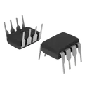
TLC555IP
555 Type, Timer/Oscillator (Single) IC 2.1MHz 8-PDIP The TLC555 is a CMOS monolithic timing circuit. The timer is fully compatible with CMOS, TTL, and MOS logic and operates at frequencies up to 2MHz. Because of a high input impedance, this device supports smaller timing capacitors than those supported by the NE555 or LM555. As a result, more accurate time delays and oscillations are possible. Power consumption is low across the full range of power-supply voltage. • Very low power consumption: – 1mW typical at VDD = 5V • Capable of operation in astable mode • CMOS output capable of swinging rail to rail • High output current capability – Sink: 100mA typical – Source: 10mA typical • Output fully compatible with CMOS, TTL, and MOS • Low supply current reduces spikes during output transitions • Single-supply operation from 2V to 15V • Functionally interchangeable with the NE555; has same pinout • ESD protection exceeds 1000V per ANSI/ESDA/ JEDEC JS-001 • Available in Q-temp automotive – High-reliability automotive applications – Configuration control and print support – Qualification to automotive standards #CommonPartsLibrary #IntegratedCircuit
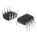
116 Uses0 StarsTLC555CP
555 Type, Timer/Oscillator (Single) IC 2.1MHz 8-PDIP Like the NE555, the TLC555 has a trigger level equal to approximately one-third of the supply voltage and a threshold level equal to approximately two-thirds of the supply voltage. These levels can be altered by use of the control voltage terminal (CONT). When the trigger input (TRIG) falls below the trigger level, the flip-flop is set and the output goes high. If TRIG is above the trigger level and the threshold input (THRES) is above the threshold level, the flip-flop is reset and the output is low. The reset input (RESET) can override all other inputs and can be used to initiate a new timing cycle. If RESET is low, the flip-flop is reset and the output is low. Whenever the output is low, a low-impedance path is provided between the discharge terminal (DISCH) and GND. All unused inputs must be tied to an appropriate logic level to prevent false triggering. • Very low power consumption: – 1mW typical at VDD = 5V • Capable of operation in astable mode • CMOS output capable of swinging rail to rail • High output current capability – Sink: 100mA typical – Source: 10mA typical • Output fully compatible with CMOS, TTL, and MOS • Low supply current reduces spikes during output transitions • Single-supply operation from 2V to 15V • Functionally interchangeable with the NE555; has same pinout • ESD protection exceeds 1000V per ANSI/ESDA/ JEDEC JS-001 • Available in Q-temp automotive – High-reliability automotive applications – Configuration control and print support – Qualification to automotive standards #CommonPartsLibrary #IntegratedCircuit
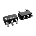
347 Uses0 StarsTPS3828-33DBVR
Supervisor Open Drain or Open Collector 1 Channel SOT-23-5 The TPS382x family of supervisors provide circuit initialization and timing supervision, primarily for DSP and processor-based systems. During power on, RESET asserts when the supply voltage VDD becomes greater than 1.1V. Thereafter, the supply voltage supervisor monitors VDD and keeps RESET active low as long as VDD remains less than the threshold voltage, VIT−. An internal timer delays the return of the output to the inactive state (high) to make sure proper system reset. The delay time, td, starts after VDD has risen above the threshold voltage (VIT− + VHYS). When the supply voltage drops below the threshold voltage VIT−, the output becomes active (low) again. No external components are required. All the devices of this family have a fixed-sense threshold voltage, VIT–, set by an internal voltage divider. The TPS382x family also offers watchdog time out options of 200ms (TPS3820) and 1.6s (TPS3823, TPS3824, and TPS3828). • Power-on reset generator with a fixed delay time of 200ms (TPS3823, TPS3824, TPS3825, and TPS3828) or 25ms (TPS3820) • Manual reset input (TPS3820, TPS3823, TPS3825, and TPS3828) • Reset output available in active-low (TPS3820, TPS3823, TPS3824, and TPS3825), active-high (TPS3824 and TPS3825), and open drain (TPS3828) • Supply voltage supervision range: 2.5V, 3V, 3.3V, 5V • Watchdog timer (TPS3820, TPS3823, TPS3824, and TPS3828) • Supply current of 15μA (typical) • 5-pin SOT-23 package • Temperature range: −40°C to 85°C (−40°C to 125°C for TPS3823A-33) #CommonPartsLibrary #IntegratedCircuit #PowerManagement #Supervisor
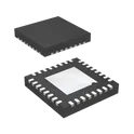
58 Uses0 StarsnRF52810-QCAA-R
IC RF TxRx + MCU Bluetooth Bluetooth v5.0 2.4GHz 32-VFQFN Exposed Pad nRF52810-QCAA-R is a multiprotocol ultra-low-power wireless System-on-Chip from Nordic Semiconductor designed for Bluetooth Low Energy and proprietary wireless communication applications. The device integrates a high-performance ARM Cortex-M processor, radio transceiver, memory resources, and peripheral interfaces into a compact package optimized for low-power embedded systems and IoT devices. This SoC supports reliable wireless connectivity with low energy consumption, making it suitable for wearable electronics, wireless sensors, smart home devices, industrial monitoring systems, and battery-powered portable applications. The integrated radio architecture provides stable RF performance with support for advanced wireless features, secure communication, and efficient coexistence in crowded RF environments. The nRF52810-QCAA-R includes multiple GPIOs, serial communication peripherals, timers, PWM functionality, analog interfaces, and low-power operating modes that simplify embedded hardware design and firmware development. Its compact package and optimized power profile make it ideal for space-constrained and energy-sensitive wireless applications. #commonpartslibrary #nordicsemiconductor #bluetoothlowenergy #wirelesssoc #iotdevices #embeddedhardware #rfdesign #lowpowerdesign #wearableelectronics #wirelesscommunication
76 Uses0 StarsBQ24074RGTT
Stand-alone single-cell linear battery charger with power path BQ24074RGTT is a highly integrated standalone linear charger and power-path management IC from Texas Instruments designed for single-cell Li-Ion/Li-Polymer battery-powered portable devices. It supports charging directly from USB ports or external adapters while simultaneously powering the system load through integrated Dynamic Power Path Management (DPPM). The device is commonly used in portable electronics, IoT devices, wireless accessories, handheld medical devices, and battery-powered embedded systems. Key Features Single-cell Li-Ion/Li-Polymer battery charger Up to 1.5 A programmable charge current Integrated Dynamic Power Path Management (DPPM) USB-compliant charging support Selectable 100 mA / 500 mA USB current limits Programmable input current limit up to 1.5 A Supports both USB input and wall adapters Input overvoltage protection up to 28 V absolute maximum Integrated thermal regulation and thermal shutdown Reverse-current and short-circuit protection Programmable pre-charge and fast-charge safety timers Battery temperature monitoring via NTC thermistor input Charge status outputs for charging/done indication Current monitoring output (ISET) Compact 16-pin VQFN (3×3 mm) package Wide operating temperature range suitable for industrial applications Typical Applications TWS charging cases and earbuds Portable medical devices IoT and asset tracking systems Handheld gaming accessories Video doorbells and IP cameras Portable embedded systems and development boards Important Design Notes Designed specifically for 1-cell battery applications Requires proper thermal PCB layout due to linear charging architecture DPPM allows the system to operate even with a deeply discharged or missing battery Recommended for compact designs needing integrated charging and system power-path control #CommonPartsLibrary #IntegratedCircuit #PowerManagement
1.2k Uses0 StarsBQ25750RRVR
Charger IC Multi-Chemistry 36-VQFN (5x6) The BQ25750RRVR is a highly integrated switch-mode battery charge controller and power-path management device designed for single-cell to multi-cell lithium-ion and lithium-polymer battery-powered systems. The device supports bidirectional power conversion, enabling both battery charging and system power delivery through USB Type-C and other DC power sources. It integrates high-efficiency buck-boost charging architecture to maintain optimal charging performance across a wide input voltage range. The device is intended for portable electronics, industrial handheld equipment, USB Power Delivery applications, embedded systems, and battery-powered computing platforms requiring advanced power management and flexible charging capability. Integrated power-path management allows simultaneous system operation and battery charging while maintaining battery protection and system stability. The BQ25750RRVR supports programmable charging parameters through an I2C interface, including charge voltage, charge current, input current limit, and system power regulation. The device includes comprehensive protection functions such as overvoltage protection, overcurrent protection, thermal regulation, battery temperature monitoring, and fault reporting. High switching frequency operation enables reduced external component size and compact PCB implementation. Features Integrated synchronous buck-boost battery charger Supports USB Power Delivery and wide DC input sources Bidirectional power conversion capability I2C programmable charging and system parameters Integrated power-path management High-efficiency charging operation Supports multi-cell lithium-ion and lithium-polymer batteries Programmable input current and charge current limits Dynamic power management and system voltage regulation Integrated ADC monitoring for voltage, current, and temperature Battery supplement mode during adapter removal OTG boost mode support Thermal regulation and thermal shutdown protection Input overvoltage and overcurrent protection Battery overvoltage protection Safety timer and watchdog timer support NTC thermistor interface for battery temperature monitoring Interrupt and fault status reporting Compact WQFN package suitable for space-constrained designs Electrical Characteristics Wide input operating voltage range Programmable battery charge voltage High charge current capability Integrated low RDS(on) MOSFET drivers High switching frequency operation High conversion efficiency across operating range Low standby and shutdown current consumption Accurate input and charge current regulation Integrated analog-to-digital converter telemetry Interface and Control I2C serial communication interface Programmable charging profiles Configurable protection thresholds Status and interrupt reporting ADC telemetry reporting Enable and control pins for system integration Protection Features Input overvoltage protection Input overcurrent protection Battery overvoltage protection Thermal shutdown protection Thermal regulation control Short-circuit protection Watchdog timer protection Safety charging timer Battery temperature qualification support Package Information Package Type: WQFN Package Suffix: RRV Compact thermally enhanced package Surface-mount device Suitable for automated PCB assembly processes Applications USB Type-C charging systems Portable computers and tablets Industrial handheld devices Power banks and battery packs Embedded battery-powered systems Portable instrumentation Consumer electronics Smart battery charging platforms #commonpartslibrary #integratedcircuit #powermanagement #batterycharger
22 Uses0 StarsBQ25622RYKR
Charger IC Lithium Ion/Polymer 18-WQFN-HR (3x2.5) The BQ25622RYKR is a highly integrated standalone switch-mode battery charge management and system power-path management device designed for single-cell lithium-ion and lithium-polymer batteries. The device integrates a high-efficiency synchronous buck charger, system power-path control, input current management, and battery protection functions into a compact solution optimized for portable and embedded applications. The device supports USB and external adapter power sources while providing programmable charging parameters through an I²C interface. Integrated power MOSFETs and advanced power management features reduce external component count and improve overall system efficiency. The charger incorporates dynamic power management, thermal regulation, battery temperature monitoring, and multiple safety protections to ensure reliable operation under varying load and environmental conditions. The BQ25622 family is designed for compact battery-powered systems requiring efficient charging, intelligent power-path control, and low system power consumption. Engineering Specification Manufacturer: Texas Instruments Device Type: Single-Cell Li-Ion/Li-Polymer Switching Battery Charger with Integrated Power-Path Management Battery Chemistry Support: Lithium-Ion and Lithium-Polymer Charging Topology: Synchronous Buck Switching Charger Input Power Sources: USB Input and External DC Adapter Support Charge Current Capability: Programmable Fast Charge Current Support Communication Interface: I²C Serial Communication Interface Integrated Power Devices: Internal High-Side and Low-Side MOSFETs Charging Features: Precharge Mode Fast Charge Mode Charge Termination Automatic Recharge Programmable Charge Parameters Safety Timer Control Power Management Features: Dynamic Power-Path Management Input Current Optimization Narrow Voltage DC Regulation Input Voltage Regulation System Voltage Regulation Monitoring and Reporting Features: Charge Status Monitoring Fault Status Reporting Battery Temperature Monitoring through NTC Interface Input Source Detection Protection Features: Input Overvoltage Protection Battery Overvoltage Protection Thermal Shutdown Protection Thermal Regulation Input Current Limiting Short-Circuit Protection Safety Timer Protection Package Type: WQFN Package Package Variant: RYK Mounting Type: Surface Mount Typical Applications: Portable Consumer Electronics Embedded Battery-Powered Devices IoT Systems Handheld Industrial Equipment USB-Powered Systems Wearable Electronics Portable Medical Devices #commonpartslibrary #integratedcircuit #powermanagement #batterycharger
7 Uses0 StarsBQ25620RYKR
Charger IC Lithium Ion/Polymer 18-WQFN-HR (3x2.5) The BQ25620RYKR is a highly integrated standalone switch-mode battery charge management and system power-path management device designed for single-cell lithium-ion and lithium-polymer batteries. The device integrates a synchronous buck charger, power-path management, input current optimization, and system regulation functions into a compact package suitable for portable and battery-powered embedded systems. It supports USB and adapter power sources with high-efficiency charging operation and dynamic power management for optimized thermal and power performance. The device includes integrated MOSFETs, charge termination, safety timers, input overvoltage protection, thermal regulation, and battery temperature monitoring. It supports I²C communication for programmable charging parameters, system monitoring, and fault reporting. The integrated narrow-voltage DC architecture improves efficiency while reducing external component count and PCB area. Engineering Specification Manufacturer: Texas Instruments Device Type: Single-Cell Li-Ion/Li-Polymer Switching Battery Charger with Power-Path Management Battery Chemistry Support: Lithium-Ion and Lithium-Polymer Charging Topology: Synchronous Buck Converter Input Supply Support: USB Power and External Adapter Sources Input Voltage Operating Range: Wide Input Voltage Support with Input Overvoltage Protection Charge Current Capability: High Current Fast Charging Support System Power Path: Integrated Dynamic Power-Path Management Communication Interface: I²C Serial Interface Integrated MOSFETs: High-Side and Low-Side Power MOSFETs Included Charging Functions: Preconditioning Charge Fast Charge Charge Termination Recharge Function Safety Timer Control Protection Features: Input Overvoltage Protection Battery Overvoltage Protection Thermal Shutdown Thermal Regulation Charge Safety Timer Input Current Limiting Short-Circuit Protection Battery Monitoring Features: Battery Temperature Monitoring via NTC Charge Status Reporting Fault Status Reporting System Voltage Regulation Power Management Features: Narrow Voltage DC Regulation Dynamic Input Power Management Input Current Optimization Automatic Power Source Detection Package Type: WQFN Package Package Variant: RYK Mounting Type: Surface Mount Application Areas: Portable Electronics Embedded Battery-Powered Systems Handheld Devices USB-Powered Equipment Industrial Portable Devices IoT Systems Consumer Electronics #commonpartslibrary #integratedcircuit #powermanagement #batterycharger
5 Uses0 StarsMAX77962EWJ12+T
Charger IC Lithium Ion 49-WLP (3.46x3.46) The MAX77962 is a high-performance wide-input 3.2A buck-boost charger with a Smart Power Selector™ and operates as a reverse buck without an additional inductor, allowing the IC to power USB On-the-Go (OTG) accessories. The device integrates low-loss power switches, and provides small solution size, high efficiency, low heat, and fast battery charging. The reverse buck has true-load disconnect and is protected by an adjustable output current limit. The device is highly flexible and programmable through I2C configuration or autonomously through resistor configuration. The battery charger includes a Smart Power Selector to accommodate a wide range of battery sizes and system loads. The Smart Power Selector allows the system to start up gracefully when an input source is available even when the battery is deeply discharged (dead battery) or missing. For battery safety/authentication reasons, the IC can be configured to keep charging disabled, and allow the DC-DC to switch and regulate the SYS voltage. The system processor can later enable charging using the appropriate I2C commands. Alternatively, the IC can be configured to automatically start charging. ● 3.5V to 23V Input Operating Range, 30VDC Withstand Voltage ● 97% Peak Efficiency at 9VIN/7.4VOUT/1.5AOUT ● Reverse Leakage Protection ● 50mA to 3.15A Programmable Input Current Limit ● 50mA to 3.2A Programmable Constant Current Charge ● Remote Differential Voltage Sensing ● 600kHz or 1.2MHz Switching Frequency Options ● System Instant On with Smart Power Selector PowerPath ● Charge Safety Timer ● Die Temperature Regulation with Thermal Foldback Loop ● Input Power Management with Adaptive Input Current Limit (AICL) and Input Voltage Regulation ● 10mΩ BATT to SYS Switch, Up to 10A Overcurrent Threshold ● Reverse Buck Mode 5.1V/1.5A to Support USB OTG ● JEITA Compliant with NTC Thermistor Monitor ● I 2C or Resistor Programmable ● 3.458mm x 3.458mm 49-Bump WLP #CommonPartsLibrary #IntegratedCircuit #PowerManagement #MAX77962
0 Uses0 StarsTPS259850RQPR
Electronic Fuse Regulator High-Side 60A 26-VQFN-HR (5x4.5) The TPS259850RQPR is an integrated eFuse power protection device designed for robust power path management in low-voltage DC systems. Manufactured by Texas Instruments, this device provides advanced protection features including overvoltage protection, undervoltage protection, overcurrent limiting, short-circuit protection, reverse current blocking, and thermal shutdown. The device is optimized for applications requiring controlled inrush current, fault isolation, and system reliability in industrial, automotive, telecommunications, and embedded electronic systems. The TPS259850RQPR supports a wide operating input voltage range and integrates programmable protection thresholds to allow flexible system-level configuration. The device includes an internal MOSFET with low on-resistance for efficient power delivery while minimizing power dissipation. Fast fault response and automatic retry functionality enhance system robustness and reduce the need for external supervisory circuitry. The device is housed in a compact QFN package suitable for space-constrained PCB designs and supports high-current operation with efficient thermal performance. The integrated protection architecture simplifies power subsystem design while improving reliability and fault tolerance. Electrical Characteristics Input operating voltage range supports low-voltage DC power rails commonly used in embedded and industrial systems. Integrated low-RDS(on) MOSFET minimizes conduction losses and improves overall efficiency. Programmable current limiting enables configurable overcurrent protection. Fast short-circuit response protects downstream circuitry during fault events. Adjustable overvoltage and undervoltage thresholds allow flexible supply monitoring. Reverse current blocking prevents back-drive conditions and protects power sources. Thermal shutdown protection disables the device during excessive junction temperature conditions. Controlled output slew rate limits inrush current during startup and hot-plug events. Automatic retry and latch-off fault management modes are supported. Power-good indication output provides system power status monitoring. Protection Features Overcurrent protection with programmable current limit threshold. Short-circuit protection with rapid fault response. Input overvoltage protection. Input undervoltage lockout protection. Reverse current and reverse polarity protection support. Thermal shutdown with automatic recovery capability. Fault timer control for transient fault management. Safe hot-swap and hot-plug operation support. Mechanical Characteristics Package type is QFN with compact footprint optimized for high-density PCB layouts. Surface-mount device compatible with automated assembly processes. Thermally enhanced package construction improves heat dissipation. RoHS-compliant and suitable for lead-free manufacturing processes. Applications Industrial power distribution systems. Automotive electronic subsystems. Telecommunication and networking equipment. Server and storage platforms. Hot-swappable modules. USB Type-C and power delivery systems. Embedded computing platforms. FPGA and processor power rail protection. Battery-powered and portable electronic equipment. #commonpartslibrary #integratedcircuit #powermanagement #regulator
7 Uses0 Stars