Timers and RTCs
Timers and Real-Time Clocks (RTCs) are electronic devices that are used to measure time or keep track of the current time. They can be found in a wide range of applications, including computers, phones, and appliances. Timers are used to trigger an action after a specific period of time has elapsed. They can be used to control the duration of an event, or to schedule tasks to be performed at a later time. RTCs, on the other hand, are used to maintain accurate time even when the device is powered off. They are often used in devices that need to keep track of the current time and date, such as alarm clocks and smart thermostats. If you're looking for high-quality timers and RTCs for your electronic projects, you should check out Flux.ai. They have the world's largest community-driven public library of timers and RTCs, with footprints, symbols, datasheets, and simulation models. This makes it easy for you to find the components you need for your project, and ensures that you have access to accurate and up-to-date information about each component. Whether you're a professional engineer or a hobbyist, Flux.ai has the resources you need to get your project off the ground.
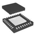
STM32G071K8U6
STM32U073 Series – ultra-low-power 32-bit microcontroller based on the Arm Cortex-M0+ core operating up to 56 MHz. Features up to 256 KB Flash memory, 40 KB SRAM, USB Full-Speed interface, integrated LCD controller, advanced analog peripherals, and extremely low power consumption. Designed for battery-powered, portable, industrial, smart metering, IoT, wearable, medical, and consumer electronics applications. Includes ADC, DAC, op-amp, comparators, RTC, DMA, timers, communication interfaces, and multiple low-power operating modes. Search Keywords: STM32U073, STM32U073RBT6, STM32U073CBT6, STM32U073 MCU, STMicroelectronics MCU, Cortex-M0+ Microcontroller, Ultra Low Power MCU, ARM Microcontroller, USB Microcontroller, LCD Controller MCU, Battery Powered MCU, Embedded Controller, IoT Microcontroller, Industrial MCU, Smart Meter MCU, Wearable MCU, 256KB Flash MCU, 40KB SRAM MCU, Low Power Embedded System, STM32U0 Series Hashtags: #STM32U073 #STM32U0 #STM32 #STMicroelectronics #CortexM0Plus #ARMMCU #Microcontroller #UltraLowPower #EmbeddedSystems #USBMCU #LCDController #IoT #WearableElectronics #SmartMeter #IndustrialElectronics #BatteryPowered #FirmwareDevelopment #ElectronicsDesign #PCBDesign #EmbeddedHardwareST Microelectronics STM32G071K8U6 UFQFPN-32_L5.0-W5.0-P0.50-TL-EP3.5 LCSC Part Number: C724237 JLCPCB Part Class: Extended Part Manufactured by ST(意法半导体)
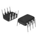
5 Uses0 StarsICM7555IPA+
Timer ICM7555IPA+ DIP-8_L10.1-W6.3-P2.54-LS7.6-BL LCSC Part Number: C1520201 ICM7555 / ICM7556 CMOS Precision Timer – low-power general-purpose timer IC compatible with the classic 555 timer architecture. Available as a single timer (ICM7555) or dual timer (ICM7556). Designed for accurate timing, pulse generation, pulse-width modulation (PWM), frequency generation, delay circuits, oscillators, and sequential timing applications. Features ultra-low supply current, wide operating voltage range (2 V to 18 V), TTL compatibility, adjustable duty cycle, and improved CMOS performance compared to standard bipolar 555 timers. Search Keywords: ICM7555, ICM7556, CMOS 555 Timer, Precision Timer IC, Low Power Timer, General Purpose Timer, PWM Generator, Pulse Generator, Oscillator IC, Delay Timer, Monostable Multivibrator, Astable Multivibrator, Frequency Generator, Timing Circuit, CMOS Timer, Analog Timer IC, Low Power Oscillator, Dual Timer IC, Single Timer IC, 555 Compatible Timer Hashtags: #ICM7555 #ICM7556 #CMOS555 #555Timer #TimerIC #PrecisionTimer #PulseGenerator #PWMGenerator #OscillatorIC #FrequencyGenerator #DelayCircuit #Monostable #Astable #CMOS #LowPowerElectronics #AnalogIC #EmbeddedSystems #ElectronicsDesign #CircuitDesign #PCBDesign
16 Uses0 StarsTPS48160QRGERQ1
TPS4816-Q1 is an automotive-qualified high-side switch controller from Texas Instruments designed for intelligent power distribution, battery management, DC/DC converter protection, and automotive power systems. Supporting operating voltages from 3.5 V to 95 V (100 V absolute maximum), the device drives external N-channel MOSFETs and provides advanced protection, diagnostics, and bidirectional current monitoring. Integrated features include overcurrent protection with programmable circuit breaker timer (I²t), fast short-circuit protection, undervoltage and overvoltage protection, reverse polarity protection down to -60 V, gate pre-charge circuitry for capacitive loads, temperature monitoring, and fault diagnostics. The controller is optimized for 12 V, 24 V, and 48 V automotive architectures, offering low standby current, high reliability, and robust protection for power distribution and battery-connected systems. Search Keywords: TPS4816-Q1, TPS4816Q1, Texas Instruments TPS4816, High Side Switch Controller, Automotive High Side Driver, Smart High Side Switch, MOSFET Controller, Battery Protection Controller, Automotive Power Distribution, Electronic Fuse Controller, eFuse Controller, Reverse Polarity Protection IC, Bidirectional Current Monitor, I2t Protection Controller, Automotive Power Management IC, 48V Automotive System, DC DC Converter Protection, Battery Management System Controller, High Voltage Switch Controller, Automotive Diagnostics IC Hashtags: #TPS4816Q1 #TexasInstruments #HighSideSwitch #SmartSwitch #AutomotiveElectronics #PowerDistribution #BatteryManagement #PowerManagement #MOSFETDriver #EFuse #CircuitProtection #CurrentMonitoring #AutomotivePower #DCDCConverter #EmbeddedSystems #PowerElectronics #ElectronicsDesign #PCBDesign #HardwareEngineering #ElectricalEngineering
11 Uses0 StarsSTM32H743VIT6
ARM® Cortex®-M7 STM32H7 Microcontroller IC 32-Bit 480MHz 2MB (2M x 8) FLASH 100-LQFP (14x14) # STM32H743VIT6 ## General Description The STM32H743VIT6 is a high-performance microcontroller manufactured by STMicroelectronics and based on the Arm Cortex-M7 core. It is designed for advanced embedded applications requiring exceptional processing capability, extensive peripheral integration, high-speed memory access, and real-time control performance. The device combines powerful computational resources, floating-point processing, digital signal processing capabilities, large embedded memory, and a comprehensive set of communication interfaces within a compact package. Its architecture is optimized for industrial automation, motor control, human-machine interfaces, medical devices, robotics, data acquisition systems, audio processing, edge computing, and high-performance IoT applications. ## Key Features ### Processing Architecture * Arm Cortex-M7 processor core * High-performance real-time processing capability * Floating-point unit support * Digital signal processing functionality * Advanced instruction set architecture * Optimized embedded computing performance ### Memory Resources * Embedded Flash memory * High-speed SRAM architecture * Memory protection support * Efficient code and data execution * High-bandwidth memory access capability * Advanced cache architecture ### Communication Interfaces * USART and UART communication interfaces * SPI communication interfaces * I²C communication interfaces * CAN communication support * USB connectivity capability * Ethernet networking support * SDMMC storage interface support * Flexible external communication options ### Analog Features * High-resolution analog-to-digital conversion * Digital-to-analog conversion capability * Precision signal acquisition * Analog monitoring functionality * Sensor interface compatibility ### Timer and Control Features * Advanced control timers * General-purpose timers * PWM signal generation * Encoder interface support * Motor-control functionality * Real-time clock integration * Event-driven control architecture ### Multimedia and Processing Capabilities * Audio processing support * Signal processing applications * Graphics and display interface support * High-speed data acquisition capability * Real-time analytics support * Edge computing functionality ### Power Characteristics * Optimized performance-to-power ratio * Multiple low-power operating modes * Dynamic power management support * Efficient embedded system operation ### Package Characteristics * Surface-mount package construction * Industrial-grade packaging * High-pin-count peripheral integration * Automated assembly compatible * Suitable for complex embedded designs ### Material Construction * Advanced semiconductor technology * RoHS-compliant materials * Lead-free package construction * High-reliability integrated circuit design ### Environmental Characteristics * Suitable for industrial and commercial environments * Long operational service life * Reliable continuous operation * Stable performance across operating conditions * Robust embedded processing platform ### Application Areas * Industrial Automation Systems * Robotics and Motion Control * Motor Drive Applications * Human-Machine Interfaces * Medical Equipment * Audio Processing Systems * Data Acquisition Equipment * Embedded Computing Platforms * Industrial Networking Devices * Edge Computing Solutions * Smart Energy Systems * Advanced IoT Devices * Test and Measurement Equipment * Consumer Electronics ### Compliance * RoHS Compliant * Lead-Free Compatible * Industrial-Grade High-Performance Microcontroller Solution ## Manufacturer STMicroelectronics ## Product Family STM32H7 High-Performance Microcontroller Series #STM32H743VIT6 #STM32H7 #STMicroelectronics #CortexM7 #Microcontroller #EmbeddedSystems #IndustrialAutomation #MotorControl #Robotics #EdgeComputing #IoT #DataAcquisition #EmbeddedDesign #FirmwareDevelopment #ElectronicsEngineering
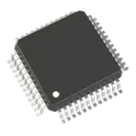
115 Uses0 StarsSTM32U083CCT6
ARM® Cortex®-M0+ STM32U0 Microcontroller IC 32-Bit 56MHz 256KB (256K x 8) FLASH 48-LQFP (7x7) # STM32U083CCT6 ## General Description The STM32U083CCT6 is an ultra-low-power microcontroller from STMicroelectronics based on the Arm Cortex-M0+ core. It is specifically designed for energy-efficient embedded applications requiring long battery life, advanced peripheral integration, secure operation, and reliable real-time performance. The device combines low-power processing, embedded Flash memory, SRAM, analog peripherals, communication interfaces, and hardware security features within a compact package. Its architecture makes it ideal for smart sensors, industrial monitoring systems, medical devices, wearable electronics, smart metering, home automation products, and Internet of Things applications where power efficiency is a primary design requirement. ## Key Features ### Processing Architecture * Arm Cortex-M0+ processor core * Optimized low-power computing architecture * Efficient real-time processing capability * Interrupt-driven operation support * Embedded system control functionality ### Memory Resources * Embedded Flash memory * Integrated SRAM * Non-volatile data storage support * High-reliability memory architecture * Efficient code execution capability ### Low-Power Features * Ultra-low-power operating modes * Multiple sleep and standby modes * Fast wake-up capability * Battery-powered application optimization * Energy-efficient peripheral operation * Extended product operating life in portable systems ### Security Features * Hardware security mechanisms * Memory protection functionality * Secure firmware execution support * Data integrity protection * Secure embedded application development support ### Communication Interfaces * USART communication interfaces * UART communication support * SPI serial communication interfaces * I²C communication interfaces * Low-power communication capability * Flexible external device connectivity ### Analog Features * Analog-to-digital conversion capability * Precision signal acquisition support * Integrated analog peripherals * Sensor interface compatibility * Low-power analog operation ### Timer and Control Functions * General-purpose timers * PWM signal generation * Real-time clock functionality * Event-driven control capability * Timing and scheduling support ### Package Characteristics * Surface-mount package * Compact footprint design * Automated assembly compatibility * Suitable for space-constrained applications * Industrial-grade packaging ### Material Construction * Advanced low-power semiconductor technology * RoHS-compliant materials * Lead-free package construction * High-reliability integrated circuit design ### Environmental Characteristics * Suitable for industrial and commercial environments * Long operational service life * Stable performance under continuous operation * Robust low-power architecture ### Application Areas * Internet of Things Devices * Smart Sensors * Wearable Electronics * Medical Monitoring Equipment * Home Automation Systems * Smart Metering Applications * Battery-Powered Products * Environmental Monitoring Systems * Industrial Data Acquisition Equipment * Consumer Electronics * Portable Embedded Systems * Wireless Sensor Nodes ### Compliance * RoHS Compliant * Lead-Free Compatible * Industrial-Grade Embedded Microcontroller Solution ## Manufacturer STMicroelectronics ## Product Family STM32U0 Ultra-Low-Power Microcontroller Series #STM32U083CCT6 #STM32U0 #STMicroelectronics #Microcontroller #UltraLowPowerMCU #CortexM0Plus #EmbeddedSystems #IoT #SmartSensors #WearableElectronics #BatteryPoweredDevices #IndustrialElectronics #EmbeddedDesign #FirmwareDevelopment #ElectronicsEngineering
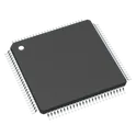
1 Uses0 StarsSTM32H573ZIT6
ARM® Cortex®-M33 STM32H5 Microcontroller IC 32-Bit 250MHz 2MB (2M x 8) FLASH 144-LQFP (20x20) # STM32H573ZIT6 ## General Description The STM32H573ZIT6 is a high-performance microcontroller from STMicroelectronics based on the Arm Cortex-M33 core. It is designed to deliver advanced processing capability, enhanced security, and extensive peripheral integration for industrial, medical, consumer, communications, and embedded control applications. The device combines powerful computational performance with low-power operation, making it suitable for real-time control, edge computing, human-machine interfaces, industrial automation, IoT gateways, motor control systems, and secure connected devices. Integrated security features, high-speed memory architecture, and comprehensive communication interfaces enable the development of robust and scalable embedded solutions. ## Key Features ### Processing Architecture * Arm Cortex-M33 processor core * TrustZone security architecture * Digital signal processing capabilities * Floating-point computation support * Optimized real-time processing performance ### Memory Resources * Embedded Flash memory * Integrated SRAM architecture * Error correction capability for enhanced reliability * High-speed memory access structure ### Security Features * Secure boot functionality * Hardware cryptographic accelerators * Secure firmware update support * Memory protection mechanisms * Tamper detection capabilities * Trusted execution environment * Secure key management support ### Communication Interfaces * USART and UART communication interfaces * SPI serial communication interfaces * I²C communication interfaces * CAN FD connectivity * USB connectivity support * Ethernet interface capability * SDMMC memory card interface * Flexible external communication options ### Analog Features * High-performance analog-to-digital conversion * Digital-to-analog conversion capability * Analog comparators * Precision signal acquisition support ### Timer and Control Functions * Advanced control timers * General-purpose timers * PWM generation capability * Encoder interface support * Motor-control functionality * Real-time clock integration ### Power Characteristics * Low-power operating modes * Dynamic power optimization * Battery-powered application support * Efficient performance-to-power ratio ### Package Characteristics * LQFP package construction * Surface-mount technology compatibility * Industrial-grade mechanical design * Suitable for automated assembly processes ### Application Areas * Industrial Automation Systems * Motor Control Equipment * Human-Machine Interfaces * Smart Energy Systems * Medical Electronics * IoT Gateways * Secure Embedded Devices * Industrial Networking Equipment * Building Automation Systems * Consumer Electronics * Data Acquisition Systems * Edge Computing Applications ### Compliance * RoHS Compliant * Lead-Free Compatible * Industrial and Commercial Application Support ## Manufacturer STMicroelectronics ## Product Family STM32H5 Series High-Performance Microcontrollers #STM32H573ZIT6 #STM32H5 #STMicroelectronics #CortexM33 #Microcontroller #EmbeddedSystems #IndustrialAutomation #SecureMCU #IoT #EdgeComputing #MotorControl #EmbeddedDesign #ElectronicsEngineering #FirmwareDevelopment #IndustrialElectronics
7 Uses0 StarsS32K358GHT1MJBST
ARM® Cortex®-M7 S32K3 Microcontroller IC 32-Bit Tri-Core 240MHz 8MB (8M x 8) FLASH 289-LFBGA (14x14) ## Engineering Specification ## General Description The **S32K358GHT1MJBST** is an NXP Semiconductors **S32K3 series automotive microcontroller** designed for high-performance embedded control applications in automotive, industrial, and electrically harsh environments. It is built around an **Arm Cortex-M7 architecture** and provides high processing capability, large embedded flash memory, automotive-grade qualification, security support, and a broad set of communication interfaces. The device is suitable for body control, gateway systems, vehicle networking, motor control, domain control, safety-related embedded systems, and general-purpose automotive electronic control units. ## Device Identification Manufacturer Part Number: **S32K358GHT1MJBST** Manufacturer: **NXP Semiconductors** Product Family: **S32K3** Device Category: **Integrated Circuit** Device Type: **Automotive Microcontroller** Core Architecture: **Arm Cortex-M7** Processing Class: **Thirty-Two-Bit MCU** Qualification: **Automotive Grade, AEC-Q100** ## Functional Description The device functions as a high-performance automotive microcontroller for embedded control and communication systems. It provides processing resources for real-time control, communication management, diagnostics, security handling, and system-level application logic. The microcontroller is designed for scalable automotive platforms where software reuse, safety capability, and peripheral integration are important. ## Core and Processing Description The **S32K358GHT1MJBST** uses an Arm Cortex-M7 based processing architecture with tri-core capability and high-speed operation. The core architecture supports digital signal processing, floating-point operation, interrupt handling, and real-time embedded software execution. This makes the device suitable for control systems that require strong computing performance and deterministic response. ## Memory Description The device includes large embedded flash memory for application firmware storage and integrated RAM for runtime operation, data buffering, communication stacks, and control algorithms. The memory architecture is suitable for complex embedded applications requiring large program space, diagnostics, bootloader support, and over-the-air update capability. ## Security and Safety Description The microcontroller includes hardware security support through **HSE-B security** and is intended for automotive applications where secure boot, cryptographic services, protected firmware operation, and system integrity are important. The S32K3 family also supports automotive safety-oriented development through features such as error correction, monitoring, and diagnostic capability. ## Communication and Interface Description The device supports multiple embedded communication interfaces suitable for vehicle and industrial networks. Supported interface types include CAN, Ethernet, I²C, SPI, UART, LIN, QSPI, SAI, SENT, and FlexIO. These interfaces allow the device to communicate with sensors, actuators, transceivers, memory devices, network controllers, and other electronic control units. ## Analog and Peripheral Description The microcontroller includes analog-to-digital conversion capability, timers, watchdog functions, direct memory access, serial audio support, and general-purpose input and output resources. These peripherals support sensing, control, timing, supervision, communication, and system management functions in embedded hardware designs. ## Electrical Description The device is designed for automotive low-voltage operation and supports use across a wide supply voltage range. It is intended for applications requiring reliable operation in automotive and industrial temperature environments. Proper power supply design, decoupling, reset control, clock configuration, and grounding should follow the manufacturer’s hardware design recommendations. ## Package and Mechanical Description The **S32K358GHT1MJBST** is supplied in a **surface-mount LFBGA package** with a compact ball-grid-array footprint. The package is intended for dense printed circuit board layouts requiring careful routing, controlled assembly process, thermal management, and proper solder joint reliability. ## Mounting and Assembly Description The component is intended for automated surface-mount PCB assembly using BGA-compatible manufacturing processes. PCB layout should follow the recommended footprint, ball escape routing, power-plane design, decoupling capacitor placement, thermal design, and inspection requirements for high-density automotive microcontroller assemblies. ## Application Suitability The device is suitable for automotive electronic control units, body control modules, gateway controllers, vehicle networking systems, motor control platforms, battery-related control systems, industrial controllers, safety-oriented embedded systems, and high-performance general-purpose control applications. ## Design Considerations The design should account for supply voltage range, clocking requirements, flash and RAM usage, thermal limits, package routing density, communication interface requirements, EMC performance, boot configuration, security provisioning, debugging access, software safety requirements, and compliance with automotive design guidelines. The device should not be operated beyond the manufacturer’s specified electrical, thermal, or mechanical limits. ## Hashtags #commonpartslibrary #integratedcircuit #microcontroller #automotivemcu #nxp #nxpsemiconductors #s32k3 #s32k358 #s32k358ght1mjbst #armcortexm7 #cortexm7 #thirtytwobit #automotiveelectronics #aecq100 #hsesecurity #canfd #ethernet #vehicleelectronics #embeddedhardware #embeddeddesign #ecu #gatewaycontroller #bodycontrolmodule #pcbdesign #hardwaredesign #electronicscomponents #electronicparts #componentlibrary #engineeringparts #electronicsengineering
2 Uses0 StarsR7FA6E10F2CFM#AA0
ARM® Cortex®-M33 RA6E1 Microcontroller IC 32-Bit 200MHz 1MB (1M x 8) FLASH 64-LFQFP (10x10) ## Engineering Specification ## General Description The **R7FA6E10F2CFM#AA0** is a Renesas Electronics **RA6E1 series microcontroller** designed for embedded control, industrial electronics, IoT edge devices, automation systems, and general-purpose connected applications. It is built around an **Arm Cortex-M33 processor with TrustZone support**, providing high performance, secure execution capability, and flexible integration for modern embedded designs. ## Device Identification Manufacturer Part Number: **R7FA6E10F2CFM#AA0** Manufacturer: **Renesas Electronics** Product Family: **RA Family** Series: **RA6 Series** Group: **RA6E1 Group** Device Category: **Integrated Circuit** Device Type: **Microcontroller Unit** ## Core and Processing The device uses an **Arm Cortex-M33 core** and is intended for high-performance embedded processing. It supports secure application development through TrustZone technology and is suitable for systems requiring reliable control, fast response, and efficient software execution. ## Memory Configuration The microcontroller includes program flash memory, data flash memory, and SRAM resources suitable for embedded firmware, application code, configuration storage, and runtime processing requirements. ## Package and Mechanical Description The component is supplied in an **LQFP surface-mount package**, making it suitable for compact printed circuit board layouts and standard automated assembly processes. ## Electrical and Operating Description The device is designed for low-voltage embedded systems and supports operation across an industrial temperature range. It is suitable for products requiring stable performance in controlled, commercial, or industrial operating environments. ## Communication and Interface Support The device supports common embedded communication interfaces such as USB, UART, SPI, I²C, QSPI, and CAN, allowing integration with sensors, displays, external memory, communication modules, and other peripheral devices. ## Analog and Control Features The microcontroller includes analog conversion capability, timer functions, PWM support, watchdog protection, reset monitoring, and low-voltage detection features. These functions make it suitable for control systems, monitoring equipment, and mixed-signal embedded applications. ## Security and Debug Features The device supports embedded security functions including TrustZone, unique device identification, and true random number generation. Debug and development access is supported through standard JTAG and SWD interfaces. ## Application Suitability This device is suitable for embedded controllers, IoT devices, industrial automation, metering equipment, appliance control, USB-connected products, sensor-based systems, and general electronic control applications requiring a compact and secure microcontroller solution. ## Hashtags #commonpartslibrary #integratedcircuit #microcontroller #renesas #renesaselectronics #ra6e1 #ra6series #armcortexm33 #embeddedsystems #electronicscomponents #semiconductor #mcu #iotdevices #industrialautomation #pcbdesign #electronicparts #componentlibrary #engineeringparts #hardwaredesign #electronicsengineering
0 Uses0 StarsRP2040
Raspberry Pi RP2040 dual-core Arm Cortex-M0+ microcontroller, running up to 133MHz, with 264KB on-chip SRAM, external QSPI flash support, USB 1.1 device/host controller, 30 GPIO pins, UART, SPI, I2C, PWM, ADC, timers and programmable I/O (PIO) blocks, 1.8V to 3.3V I/O support, low-cost MCU for embedded systems, development boards, IoT devices, USB peripherals, sensors and educational electronics. Search Keywords: RP2040, Raspberry Pi RP2040, RP2040 microcontroller, dual core Cortex-M0+ MCU, Raspberry Pi Pico MCU, RP2040 PIO, RP2040 USB microcontroller, RP2040 QSPI flash, RP2040 datasheet, RP2040 embedded MCU Hashtags: #RP2040 #RaspberryPiRP2040 #RaspberryPiPico #Microcontroller #CortexM0Plus RP2040 chip for Raspberry Pi Pico - ARM® Cortex®-M0+ MCU 32-Bit
2 Uses0 Stars