Memory
A memory IC, or integrated circuit, is a type of electronic device that stores and retrieves data. It is used in a wide range of electronic devices, including computers, smartphones, and other electronic devices. Memory ICs come in a variety of types, including DRAM, SRAM, and Flash memory, and are used for different purposes depending on the device and application. One of the primary use cases for memory ICs is in computer systems, where they are used to store data and instructions that are accessed by the processor. Memory ICs are also used in a variety of other electronic devices, such as digital cameras, MP3 players, and mobile phones, to store data and enable various functions. Flux.ai has the world's largest community-driven public library of memory ICs, with a wide variety of footprints, symbols, datasheets, and simulation models available. This extensive library allows users to easily access and use memory ICs in their projects, making it an invaluable resource for engineers and developers.
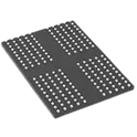
MT53E1536M32D4DT-046 WT:A
SDRAM - Mobile LPDDR4 Memory IC 48Gbit 2.133 GHz MT53E1536M32D4DT-046 WT:A is a high-density 48Gb (6GB) LPDDR4/LPDDR4X SDRAM memory device from Micron Technology. It is designed for high-performance, low-power applications requiring fast memory bandwidth and efficient power management. The device features a 32-bit data bus, supports data rates up to 4266 MT/s, and is packaged in a compact 200-ball FBGA, making it suitable for embedded computing, industrial systems, networking equipment, AI edge devices, automotive electronics, and mobile platforms. Key Features 48Gb (6GB) LPDDR4/LPDDR4X SDRAM Organized as 1.5G × 32 bits Data transfer rates up to 4266 MT/s Maximum clock frequency of 2133 MHz Low-power operation with 1.1V core supply 32-bit memory interface 200-ball FBGA package JEDEC LPDDR4-compliant architecture Per-bank refresh support Temperature-compensated refresh Self-refresh and deep power-down modes Partial-array self-refresh capability High bandwidth with reduced power consumption Optimized for compact embedded designs Operating temperature range: –30°C to +85°C Typical Applications Embedded Linux computers Single-board computers (SBCs) AI and edge computing platforms Industrial automation systems Networking and telecommunications equipment Automotive infotainment and control systems Tablets and mobile devices FPGA and SoC-based designs #commonpartslibrary #integratedcircuit #memory #dram #sdram #lpddr4 #lpddr4x #mobiledram #micron #embeddedsystems #embeddedcomputing #industrialelectronics #automotiveelectronics #edgecomputing #artificialintelligence #networking #telecommunications #highspeedmemory #lowpowerdesign #computerhardware #electroniccomponents #semiconductor #datasheet #fbga #memorychip #electronicsdesign #pcbdesign #hardwareengineering #electronicengineering #systemonchip #fpga #iot #internetofthings #computermemory #digitalelectronics #surfaceMount #smt #bga #storage #highperformancecomputing #hpc #mobiledevices #industrialautomation #electronicdesign #componentlibrary #fluxlibrary #parametricpart #eda #schematic #pcb #electronicdesignautomation #chipdesign #embeddedhardware #memorymodule #lowpowerelectronics #highbandwidthmemory #electronics #hardwaredevelopment #engineering #electricalengineering
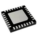
1 Uses0 StarsSTM32L432KCU6
ST Microelectronics STM32L432KCU6 UFQFPN-32_L5.0-W5.0-P0.50-TL-EP3.5 LCSC Part Number: C1337280 JLCPCB Part Class: Extended Part Manufactured by ST(意法半导体) STMicroelectronics STM32L432KC ultra-low-power 32-bit ARM Cortex-M4 microcontroller with FPU running up to 80MHz, featuring 256KB Flash memory, 64KB SRAM, USB 2.0 Full-Speed device support, Quad-SPI interface, RTC with calendar and alarms, true random number generator (TRNG), DMA controller, CAN 2.0B, UART, LPUART, SPI, I2C, SAI audio interface, 12-bit 5MSPS ADC, dual 12-bit DACs, operational amplifier with PGA, comparators, capacitive sensing channels, advanced timers and ultra-low-power modes. Operates from 1.71V to 3.6V and is optimized for battery-powered, industrial, medical, IoT and portable embedded applications. Search Keywords: STM32L432KC, STM32L432KCU6, STM32L432KCU6TR, STM32L432, STM32L4 series, STM32 Cortex-M4 MCU, STM32 low power microcontroller, STM32 256KB Flash 64KB SRAM, STM32 USB FS MCU, STM32 CAN MCU, STM32 Quad SPI MCU, STM32L432 datasheet, STM32L432 development board, Nucleo-L432KC, ARM Cortex-M4 FPU Hashtags: #STM32L432KC #STM32L432KCU6 #STM32L432 #STM32L4 #STMicroelectronics #CortexM4 #ARMMicrocontroller #LowPowerMCU #EmbeddedSystems #USBFS #CANBus #QuadSPI #ADC12bit #DAC12bit #RTC #TRNG #IoTMCU #IndustrialMCU #MedicalElectronics #NucleoL432KC
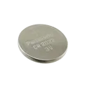
46 Uses0 StarsCR2032
Coin, 20.0mm Lithium Manganese Dioxide 3 V Battery Non-Rechargeable (Primary) The CR2032 is a compact, coin-cell lithium battery widely used in portable electronic devices, providing long-lasting, stable power in a small form factor. It features a cylindrical shape with a flat positive terminal and a metal casing that serves as the negative terminal. Known for its high energy density and wide operating temperature range, this battery is ideal for memory backup, real-time clocks, small medical devices, remote controls, wearable electronics, and low-drain consumer electronics. Its reliability, shelf life, and lightweight design make it a standard choice for a broad range of compact electronic applications. Engineering Specifications Battery Type: Lithium Coin Cell Chemistry: Lithium Manganese Dioxide Standard Designation: CR2032 Nominal Voltage: 3 Volts Capacity: Typical Rated Capacity for Consumer Electronics Discharge Characteristics: Suitable for Low-Drain Applications Dimensions: Standard Diameter and Height for CR2032 Operating Temperature Range: Wide Range for Consumer and Industrial Use Shelf Life: Extended, Suitable for Long-Term Storage Terminals: Flat Positive Top, Metal Casing Negative Bottom RoHS Compliant: Yes Applications: Watches, Calculators, Motherboard CMOS Backup, Fitness Trackers, Remote Controls, Medical Devices, Sensors, Small Electronics #CR2032 #LithiumBattery #CoinCell #3Volt #LongLifeBattery #PortableElectronics #Wearables #ConsumerElectronics #MemoryBackup #LowDrainDevice #IndustrialElectronics #BatteryComponent #PCBDesign #CompactPower
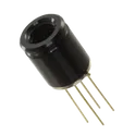
2 Uses0 StarsMLX90640ESF-BAB-000-TU
Thermal Image Sensor 32H x 24V TO-39 # MLX90640ESF-BAB-000-TU Engineering Specifications **General Description** The MLX90640ESF-BAB-000-TU is a contactless infrared thermal imaging sensor manufactured by Melexis. It incorporates a microbolometer array that detects infrared radiation emitted by objects and converts the captured thermal energy into temperature data, enabling the creation of thermal images without physical contact. The device is designed for compact and cost-effective thermal imaging applications, offering high thermal sensitivity and accurate temperature measurement capabilities. It integrates a digital signal-processing engine, calibration data memory, and a digital communication interface, allowing direct connection to microcontrollers, embedded systems, and industrial monitoring equipment. The sensor provides real-time thermal mapping across its field of view and is suitable for applications involving human presence detection, predictive maintenance, industrial automation, smart building systems, medical screening, consumer electronics, robotics, and thermal monitoring solutions. Its factory calibration ensures stable performance throughout its operating life while minimizing external calibration requirements. **Engineering Specifications** **Manufacturer:** Melexis **Manufacturer Part Number:** MLX90640ESF-BAB-000-TU **Component Type:** Infrared thermal imaging sensor **Sensor Technology:** Microbolometer thermal sensor array **Measurement Method:** Non-contact infrared temperature sensing **Output Type:** Digital thermal image data **Communication Interface:** I²C-compatible serial interface **Temperature Measurement Capability:** Object temperature monitoring and thermal imaging **Thermal Imaging Function:** Real-time thermal map generation **Integrated Processing:** On-chip signal processing and calibration management **Calibration:** Factory calibrated with stored calibration parameters **Power Supply Configuration:** Single-supply operation **Power Consumption:** Optimized for low-power embedded applications **Refresh Rate:** Programmable thermal frame refresh operation **Thermal Sensitivity:** High-sensitivity infrared detection **Field of View Variant:** Wide-angle thermal imaging configuration **Accuracy Characteristics:** High-precision temperature measurement with integrated compensation algorithms **Memory Features:** Internal EEPROM for calibration coefficients **Operating Mode:** Continuous and programmable thermal acquisition **Data Output Format:** Digital temperature and thermal pixel information **Environmental Stability:** Designed for reliable operation across varying ambient conditions **Electromagnetic Compatibility:** Suitable for embedded and industrial electronic systems **Package Type:** Surface-mount package with infrared-transparent window **Mounting Style:** Surface mount technology **Package Construction:** Reflow-solderable assembly **Lead Finish:** Lead-free finish **Environmental Compliance:** RoHS compliant and halogen-free **Reliability Features:** Factory-tested and production-calibrated thermal imaging device **Typical Applications** Thermal cameras Human presence detection systems Occupancy monitoring Industrial predictive maintenance Electrical equipment inspection Smart building automation HVAC monitoring systems Medical screening devices Consumer electronics Robotics and autonomous systems Fire detection and prevention systems Industrial process monitoring Energy management systems Automotive thermal sensing applications Security and surveillance equipment #MLX90640 #MLX90640ESF #Melexis #ThermalSensor #InfraredSensor #ThermalImaging #Microbolometer #TemperatureSensor #IndustrialAutomation #EmbeddedSystems #IoT #PredictiveMaintenance #SmartBuilding #ThermalCamera #ElectronicComponents #EngineeringSpecifications
9 Uses0 StarsADXL345TCCZ-EP
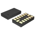
Accelerometer X, Y, Z Axis ±2g, 4g, 8g, 16g 0.05Hz ~ 1.6kHz 14-LGA (3x5) The ADXL345-EP is an extended performance version of the ADXL345, which is a small, thin, ultralow power, 3-axis accelerometer with high resolution (13-bit) measurement at up to ±16 g. Digital output data is formatted as 16-bit twos complement and is accessible through either a SPI (3- or 4-wire) or I2 C digital interface. The ADXL345-EP is well suited for extended temperature range industrial and aerospace equipment. It measures the static acceleration of gravity in tilt-sensing applications, as well as dynamic acceleration resulting from motion or shock. Its high resolution (3.9 mg/LSB) enables measurement of inclination changes less than 1.0°. Several special sensing functions are provided. Activity and inactivity sensing detect the presence or lack of motion by comparing the acceleration on any axis with user-set thresholds. Tap sensing detects single and double taps in any direction. Freefall sensing detects if the device is falling. These functions can be mapped individually to either of two interrupt output pins. An integrated memory management system with a 32-level first in, first out (FIFO) buffer can be used to store data to minimize host processor activity and lower overall system power consumption. Low power modes enable intelligent motion-based power management with threshold sensing and active acceleration measurement at extremely low power dissipation. The ADXL345-EP is supplied in a small, thin, 3 mm × 5 mm × 1 mm, 14-lead, enhanced plastic package. Ultralow power: as low as 23 µA in measurement mode and 0.1 µA in standby mode at VS = 2.5 V (typical) Power consumption scales automatically with bandwidth User-selectable resolution from 10 to 13 bits 4 mg/LSB scale factor in all g ranges 32-sample FIFO minimizes host processor load Single tap, double tap, and free-fall detection Activity/inactivity monitoring Supply voltage range: 2.0 V to 3.6 V I/O voltage range: 1.7 V to VS SPI (3- and 4-wire) and I2C digital interfaces Flexible interrupt modes mappable to either interrupt pin Measurement ranges selectable via serial command Bandwidth selectable via serial command 10,000 g shock survival Pb free/RoHS compliant Small and thin: 3 mm × 5 mm × 1 mm LGA package #CommonPartsLibrary #Sensor #Motion-sensor #accelerometer
49 Uses0 StarsSN74HCT125DRE4
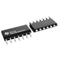
Buffers / Drivers SN74HCT125DRE4 SOIC-14_L8.6-W3.9-P1.27-LS6.0-BL LCSC Part Number: C2675588 JLCPCB Part Class: Extended Part Manufactured by TI(德州仪器) Texas Instruments SN74HCT125/SN54HCT125 quadruple bus buffer IC with 3-state outputs, contains four independent non-inverting buffers with TTL-compatible inputs, positive logic function Y=A, 4.5V to 5.5V operating voltage range, high-current outputs capable of driving up to 15 LSTTL loads, ±6mA output drive at 5V, low input current, typical 12ns propagation delay, suitable for bus line driving, memory address buffering and digital logic interface applications, available in SOIC-14 and PDIP-14 packages. Search Keywords: SN74HCT125, SN54HCT125, Texas Instruments SN74HCT125, TI SN74HCT125, SN74HCT125 buffer, 74HCT125 buffer, quad bus buffer, quadruple bus buffer, 3-state buffer IC, tri-state buffer IC, non-inverting buffer IC, TTL-compatible CMOS buffer, HCT logic buffer, bus line driver, memory address buffer, SN74HCT125D, SN74HCT125N, SOIC-14 buffer, PDIP-14 buffer, SN74HCT125 datasheet Hashtags: #SN74HCT125 #SN54HCT125 #74HCT125 #TexasInstrumentsSN74HCT125 #TIBufferIC #BusBuffer #QuadBusBuffer #TriStateBuffer #3StateBuffer #NonInvertingBuffer #HCTLogic #TTLCompatibleInput #LogicBufferIC #BusLineDriver #AddressBuffer #SOIC14 #PDIP14
45 Uses0 StarsL76KB-A58
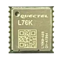
Satellite Positioning Modules L76KB-A58 GPSM-SMD_18P-L10.1-W9.7-P1.10 LCSC Part Number: C2916234 JLCPCB Part Class: Extended Part Manufactured by Quectel(移远) Quectel L76 compact GNSS module, concurrent multi-GNSS receiver supporting GPS, GLONASS, BeiDou, Galileo and QZSS, 33 tracking channels, 99 acquisition channels and 210 PRN channels, supports EASY AGPS and AlwaysLocate technology, integrated LOCUS embedded logger with internal flash memory, low power consumption, suitable for automotive, industrial PDA, consumer, industrial and portable positioning applications. Search Keywords: Quectel L76, L76 GNSS module, Quectel L76 GPS module, compact GNSS module, multi GNSS receiver, GPS GLONASS BeiDou Galileo QZSS module, L76 GPS GLONASS module, L76M33, L76 compact GPS module, Quectel GNSS receiver, GNSS module with AGPS, EASY AGPS module, AlwaysLocate GNSS, LOCUS logger GNSS module, low power GNSS module, Quectel L76 datasheet Hashtags: #QuectelL76 #L76GNSS #L76GPS #QuectelGNSS #GNSSModule #GPSModule #MultiGNSS #GPSReceiver #GLONASSModule #BeiDouModule #GalileoModule #QZSSModule #CompactGNSSModule #AGPSModule #EASYAGPS #AlwaysLocate #LOCUSLogger #LowPowerGNSS
33 Uses0 StarsESP32-C3FN4
ESP32-C3FN4 QFN-32_L5.0-W5.0-P0.50-BL-EP3.7 LCSC Part Number: C2848860 JLCPCB Part Class: Extended Part Manufactured by ESPRESSIF(乐鑫) Espressif ESP32-C3FN4 2.4GHz Wi-Fi 802.11b/g/n and Bluetooth 5.0 LE wireless SoC, RISC-V single-core microcontroller, integrated 4MB flash memory, 2.402GHz to 2.48GHz RF transceiver, antenna not included, surface-mount package, suitable for IoT devices, wireless sensors, smart home, BLE and Wi-Fi embedded applications. Search Keywords: ESP32-C3FN4, Espressif ESP32-C3FN4, ESP32 C3FN4, ESP32-C3 4MB flash, ESP32-C3 WiFi Bluetooth SoC, ESP32-C3FN4 RF transceiver, ESP32-C3FN4 Bluetooth 5.0, ESP32-C3FN4 WiFi 802.11bgn, ESP32-C3FN4 SMD, ESP32-C3FN4 DigiKey, ESP32-C3FN4 datasheet, 1904-ESP32-C3FN4TR-ND, 1904-ESP32-C3FN4CT-ND, ESP32-C3 RISC-V SoC Hashtags: #ESP32C3FN4 #ESP32C3 #EspressifESP32C3 #EspressifSystems #WiFiBluetoothSoC #WiFiSoC #BluetoothLESoC #BLE5 #80211bgn #RISCVMicrocontroller #4MBFlash #RFTransceiver #24GHzWiFi #IoTSoC #WirelessMCU
19 Uses0 StarsATTINY1616-MFR
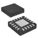
ATTINY1616-MFR QFN-20_L3.0-W3.0-P0.40-TL-EP1.7 LCSC Part Number: C1338523 JLCPCB Part Class: Extended Part Manufactured by MICROCHIP(美国微芯) Microchip ATtiny1614/1616/1617 tinyAVR 1-series 8-bit microcontroller, AVR CPU running up to 20MHz, up to 16KB self-programmable Flash memory, 256B EEPROM and 2KB SRAM, 1.8V to 5.5V operating voltage range, single-pin UPDI programming and debug interface, power-on reset and brown-out detector, internal 16/20MHz oscillator, timers, watchdog, USART, SPI, I2C/TWI, 10-bit ADC, DAC, analog comparators, event system, configurable custom logic and peripheral touch controller, available in 14-pin, 20-pin and 24-pin packages depending on variant. Search Keywords: ATtiny1614, ATtiny1616, ATtiny1617, Microchip ATtiny1614, Microchip ATtiny1616, Microchip ATtiny1617, tinyAVR 1-series, AVR 8-bit microcontroller, ATtiny 16KB Flash, ATtiny UPDI, ATtiny1616 microcontroller, ATtiny1617 MCU, ATtiny1614 MCU, 20MHz AVR microcontroller, ATtiny I2C SPI USART, ATtiny1616 datasheet, ATtiny1614 datasheet, ATtiny1617 datasheet Hashtags: #ATtiny1614 #ATtiny1616 #ATtiny1617 #MicrochipATtiny #MicrochipMCU #tinyAVR #tinyAVR1Series #AVRMicrocontroller #8bitMicrocontroller #ATtinyMCU #UPDI #16KBFlashMCU #20MHzMCU #I2CMCU #SPIMCU #USARTMCU #ADCmicrocontroller #TouchControllerMCU
60 Uses0 StarsESP32-C3-MINI-1-H4
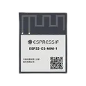
ESP32-C3-MINI-1-H4 is a compact, low-power wireless module from Espressif Systems built around the ESP32-C3 SoC. It integrates a 32-bit RISC-V processor, 2.4 GHz Wi-Fi, Bluetooth 5 LE, onboard 4 MB flash memory, crystal oscillator, RF matching circuitry, and a PCB antenna in a small surface-mount package. The module is designed for IoT devices, smart home products, industrial automation, wearable electronics, and wireless sensor applications. Key Features 32-bit RISC-V single-core processor with clock speeds up to 160 MHz. 2.4 GHz Wi-Fi 4 (802.11 b/g/n) connectivity. Bluetooth 5 Low Energy (BLE 5.0) support with long-range capability. 4 MB embedded SPI flash memory (H4 variant). 384 KB ROM and 408 KB SRAM for application execution. Integrated PCB antenna for simplified RF design. USB Serial/JTAG controller for programming and debugging without an external USB-to-UART bridge. Multiple peripheral interfaces: UART SPI I²C I²S PWM GPIO ADC USB JTAG Operating voltage range: 3.0 V to 3.6 V. Supports secure boot, flash encryption, and hardware cryptographic acceleration. Compact SMD module suitable for space-constrained designs. Typical Applications Smart home and home automation devices Wireless sensors and data loggers IoT gateways and edge devices Industrial monitoring and control systems Bluetooth beacons Wearable electronics Consumer connected products H4 Variant Note: The ESP32-C3-MINI-1-H4 version includes 4 MB flash memory and supports an extended operating temperature range up to 105°C, making it suitable for more demanding industrial environments. #RF-Transceiver #ESP32 #Module
99 Uses0 Stars