Memory
A memory IC, or integrated circuit, is a type of electronic device that stores and retrieves data. It is used in a wide range of electronic devices, including computers, smartphones, and other electronic devices. Memory ICs come in a variety of types, including DRAM, SRAM, and Flash memory, and are used for different purposes depending on the device and application. One of the primary use cases for memory ICs is in computer systems, where they are used to store data and instructions that are accessed by the processor. Memory ICs are also used in a variety of other electronic devices, such as digital cameras, MP3 players, and mobile phones, to store data and enable various functions. Flux.ai has the world's largest community-driven public library of memory ICs, with a wide variety of footprints, symbols, datasheets, and simulation models available. This extensive library allows users to easily access and use memory ICs in their projects, making it an invaluable resource for engineers and developers.
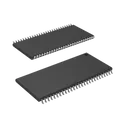
AS4C32M16SB-7TCN
SDRAM Memory IC 512Mbit Parallel 143 MHz 5.4 ns 54-TSOP II The AS4C32M16SB-7TCN is a single-data-rate synchronous dynamic random-access memory (SDR SDRAM) device manufactured by Alliance Memory. It is organized internally as a multi-bank array, allowing concurrent access operations across banks to improve effective memory bandwidth compared to simpler asynchronous DRAM architectures. The device is intended for general-purpose embedded memory applications where a synchronous, clock-driven memory interface is required, including embedded systems, industrial controllers, consumer electronics, networking equipment, and other designs that rely on a parallel SDRAM interface for working memory or buffering. As a drop-in style component within Alliance Memory's broader memory portfolio, this part is designed to be pin- and function-compatible with legacy SDR SDRAM devices originally offered by other manufacturers, allowing designers to source a continued-availability alternative for designs that depend on this memory architecture even as some original suppliers have discontinued production. This makes the device particularly useful in long-lifecycle industrial, embedded, and legacy system designs where a guaranteed supply of a specific memory interface and timing profile is critical to sustaining production over many years. The "B" designation in the part family indicates a specific die revision within the AS4C32M16S product line, reflecting a particular generation of internal silicon design while maintaining functional and pinout compatibility with related die revisions in the same footprint. The device communicates over a standard synchronous SDRAM command interface, using a clock-synchronized protocol for row and column addressing, data burst transfers, and bank management, and it supports the auto-refresh and self-refresh mechanisms typical of SDRAM devices to maintain stored data integrity without requiring constant external refresh management by the host controller. Mechanically, the device is housed in a thin small-outline package suited to space-constrained PCB layouts, and it is built for standard surface-mount assembly processes. The "-7TCN" suffix on this part number reflects a specific speed grade, package style, and temperature grade combination within the product family, with this particular variant intended for commercial temperature range operation. The device is supplied in tray packaging for surface-mount assembly and is compliant with RoHS material restrictions, supporting standard environmental and regulatory requirements for electronic components. Spec Sheet Identification Part Number: AS4C32M16SB-7TCN Device Family: AS4C32M16SB Manufacturer: Alliance Memory, Inc. Die Revision: B-die Functional Classification Device Type: Synchronous DRAM (SDR SDRAM) Memory Organization: Multi-bank array architecture Interface Type: Parallel, clock-synchronous command interface Refresh Capability: Supports auto-refresh and self-refresh modes Electrical Characteristics Supply Voltage: Standard 3.3V-class SDRAM supply rating Clock Frequency: Mid-range SDR SDRAM clock speed class Access Timing: Standard SDR SDRAM access time class for its speed grade Environmental & Qualification Temperature Grade: Commercial ("C" suffix designation) RoHS Compliance: Yes Product Positioning: Long-lifecycle, drop-in replacement memory device Package Package Type: Thin Small Outline Package, TSOP-II style Mounting: Surface mount technology (SMT) Packaging Format Supply Format: Tray packaging #AS4C32M16SB #AllianceMemory #SDRAM #SDRSDRAM #MemoryIC #EmbeddedMemory #TSOP #SurfaceMount #LegacyMemory #DropInReplacement #DRAM #EmbeddedSystems #IndustrialElectronics #SemiconductorIC #EngineeringSpec #ComponentLibrary #CommonPartsLibrary #RoHSCompliant #MemoryComponent #PCBDesign #CommonPartsLibrary #IntegratedCircuit #Memory #AS4C32
15 Uses0 StarsIRLR7843TRPBF
N-Channel 30 V 161A (Tc) 140W (Tc) Surface Mount TO-252AA (DPAK) The IRLR7843TRPBF is an N-channel power MOSFET built on Infineon's HEXFET technology platform, originally developed by International Rectifier. It is designed as a low-voltage, high-current switching device intended for applications where minimizing conduction loss and maximizing efficiency are primary design goals. The part is particularly well suited to synchronous switching topologies, where pairs or arrays of MOSFETs alternately conduct to regulate power flow with minimal energy dissipation. This device targets high-density power conversion applications where board space is limited but current demands are substantial, such as notebook computer power delivery, point-of-load converters used in servers, and advanced telecom and datacom equipment. It is commonly found supporting synchronous buck converter stages that step down a higher input rail to a lower output voltage suitable for powering processors, memory, and other low-voltage digital logic. Its low on-resistance characteristic allows it to carry significant current while generating comparatively little resistive heating, which is essential in compact enclosures with constrained thermal budgets. The transistor is fabricated using a refined trench gate process that improves upon earlier HEXFET generations, offering reduced gate charge and lower switching losses alongside its low conduction resistance. This combination makes it effective in both the high-side and low-side positions of a synchronous switching cell, where fast, clean transitions reduce overlap losses and improve overall converter efficiency. The device also offers well-characterized avalanche energy ratings, giving designers confidence in its ruggedness when exposed to transient overvoltage events that can occur during switching, and it presents a very low gate impedance, allowing it to be driven efficiently by standard gate driver circuitry. Mechanically, the part is housed in a surface-mount power package with an exposed tab for enhanced thermal conduction to the host PCB, allowing heat generated during operation to be efficiently transferred away from the silicon die. This package style is widely used in power-dense designs where through-hole packages would be impractical. The device is supplied in a tape-and-reel format suitable for automated assembly and is compliant with RoHS material restrictions, reflecting current environmental and regulatory standards for electronic components. Spec Sheet Identification Part Number: IRLR7843TRPBF Device Family: HEXFET Power MOSFET Manufacturer: Infineon Technologies Functional Classification Device Type: Power MOSFET Channel Type: N-channel Technology: Trench-gate HEXFET (IR MOSFET legacy technology) Logic Level Compatibility: Logic-level gate drive compatible Electrical Characteristics Drain-to-Source Voltage Rating: Low-voltage class, optimized for sub-30V rail applications On-Resistance: Ultra-low on-resistance class Drain Current Capability: High continuous current class Gate Charge: Low gate charge, optimized for fast switching Gate Impedance: Ultra-low gate impedance Avalanche Characteristics: Fully characterized avalanche voltage and current rating Switching & Application Behavior Primary Application: Synchronous buck converter switching stages Suitable Position: High-side and low-side switch positions Target Use Cases: Point-of-load conversion, notebook power delivery, telecom/datacom power systems Thermal & Mechanical Package Type: Surface-mount power package with exposed thermal tab (DPAK-style) Mounting: Surface mount technology (SMT) Thermal Path: Tab-based conduction to PCB for heat dissipation Environmental & Qualification RoHS Compliance: Yes Lifecycle Status: Active production Packaging Format Supply Format: Tape-and-reel, per part suffix designation #IRLR7843 #Infineon #HEXFET #PowerMOSFET #NChannelMOSFET #SynchronousBuck #PowerElectronics #DCDCConverter #PointOfLoad #PowerConversion #DPAK #SMTPackage #RoHSCompliant #SemiconductorIC #EngineeringSpec #ComponentLibrary #CommonPartsLibrary #PowerDensity #LowRDSon #DiscreteSemiconductor #commonpartslibrary #transistor
3 Uses0 StarsLAN9254-I/JRX
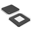
Ethernet Controller 10/100 Base-T/TX Bus Interface 80-TQFP-EP (12x12) The LAN9254-I/JRX is an EtherCAT SubDevice (slave) controller developed by Microchip Technology, designed to serve as the communication backbone for industrial automation devices participating in an EtherCAT network. The device integrates dual Ethernet physical layer transceivers directly on-chip, eliminating the need for external PHY components and simplifying the design of EtherCAT-enabled equipment such as servo drives, sensors, I/O modules, and other field devices used in real-time industrial control systems. Architecturally, the controller can operate as either a two-port or three-port node, depending on the network topology required. In its standard configuration it functions as a two-port device supporting daisy-chain connections typical of EtherCAT line topologies. When configured as a three-port device, it gains an additional management interface port that can connect to an external PHY or to another LAN9254, enabling star or tree network topologies and allowing the device to act as a branching point within a larger EtherCAT installation. Each integrated Ethernet PHY operates in full-duplex mode and supports automatic crossover detection, so the device can use either straight-through or crossover cabling without requiring manual configuration. Beyond pure protocol handling, the LAN9254 includes a substantial set of general-purpose digital input and output lines, allowing it to be used in simple field devices without requiring a separate microcontroller. For more complex applications, the device communicates with an external host processor through an integrated host bus interface that behaves like simple memory-mapped SRAM, supporting both 8-bit and 16-bit data widths along with multiple byte-ordering conventions, which makes it straightforward to interface with a wide range of microcontroller and microprocessor architectures. Internally, dual process data RAM buffers manage the exchange of real-time process data between the host application and the EtherCAT communication engine, while a dedicated interrupt line notifies the host of relevant internal events. A key feature of the device is its built-in distributed clock mechanism, which provides high-precision timing synchronization across all nodes in an EtherCAT network. This capability is essential for motion control and other applications where multiple devices must act in tight temporal coordination. The controller also provides configurable status indication through standard network activity and link LEDs, along with optional error and run-state indicators that give visibility into the health and operational state of the device at a glance. Power architecture on the LAN9254 is simplified through an integrated linear regulator, allowing the device to be operated from a single primary supply rail while internally generating the lower voltage needed for its core logic. This reduces the external power supply complexity that would otherwise be required to support separate core and I/O voltage domains. The "-I" designation on this particular part number indicates an industrial-grade temperature rating, making it suitable for deployment in factory floor and other demanding industrial environments where extended thermal range and long-term reliability are required. The device is housed in a surface-mount package consistent with dense industrial control board layouts and is compliant with RoHS material restrictions. Spec Sheet Identification Part Number: LAN9254-I/JRX Device Family: LAN9254 Manufacturer: Microchip Technology Functional Classification Device Type: EtherCAT SubDevice (slave) controller Network Role: Two/three-port configurable node Integrated PHYs: Dual Ethernet physical layer transceivers, on-chip Auto-MDIX Support: Yes, supports direct and crossover cabling Communication & Protocol Features Protocol: EtherCAT Topology Support: Daisy-chain (line), star, and tree topologies Additional Port Mode: Optional third port for branching/tap configurations Clock Synchronization: Integrated distributed clock for high-precision timing Host Interface Interface Type: SRAM-like host bus interface Data Width Support: Selectable bit-width host bus operation Endianness Support: Multiple byte-ordering modes Process Data Handling: Dual process data RAM buffers Interrupt Support: Configurable host interrupt line Digital I/O General-Purpose I/O: Integrated digital I/O lines for microcontroller-less operation Standalone Mode: Supports operation without external microcontroller for simple device designs Power Architecture Supply Configuration: Single primary supply rail Internal Regulation: Integrated linear regulator for core voltage generation Status Indication LED Support: Standard run and link/activity indicators per port Optional Indicators: Configurable error and run-state status indicators Environmental & Qualification Temperature Grade: Industrial ("-I" suffix) RoHS Compliance: Yes Package Package Type: Surface-mount, quad flat package style Mounting: Surface mount technology (SMT) Packaging Format Supply Format: Tape-and-reel, per part suffix designation #LAN9254 #Microchip #EtherCAT #SlaveController #SubDeviceController #IndustrialEthernet #IndustrialAutomation #MotionControl #EmbeddedSystems #FieldDevice #DigitalIO #HostBusInterface #DistributedClock #TQFP #RoHSCompliant #IndustrialGrade #EngineeringSpec #ComponentLibrary #CommonPartsLibrary #SemiconductorIC
1 Uses0 StarsW25Q02JVSFIM
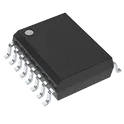
The W25Q02JVSFIM from Winbond Electronics is a 2G-bit (256M x 8) Serial NOR Flash Memory device designed for high-density non-volatile data storage applications. It supports high-speed SPI, Dual/Quad SPI, QPI, and DTR interfaces, providing fast data transfer and efficient memory access for embedded systems. The device operates from a 2.7V to 3.6V supply voltage and is available in a 16-pin SOIC surface-mount package. It is suitable for applications such as firmware storage, boot code memory, industrial controllers, IoT devices, automotive electronics, and embedded systems requiring large-capacity reliable flash memory. Key Features Memory Density: 2G-bit Serial NOR Flash (256M x 8) Flash Technology: Single-Level Cell (SLC) NOR Flash Interface Support: Standard SPI, Dual SPI, Quad SPI, QPI, and DTR modes High-Speed Clock Frequency: Up to 133 MHz operation Fast Access Time: Approximately 7.5 ns Supply Voltage Range: 2.7V to 3.6V Non-Volatile Data Storage: Retains stored data without power Memory Organization: 256M x 8-bit architecture Package Type: 16-pin SOIC (7.50 mm width) surface-mount package Operating Temperature Range: -40°C to +85°C Page Program Time: Approximately 3.5 ms Applications: Embedded firmware storage, BIOS/boot memory, industrial equipment, IoT devices, and consumer electronics Hashtags #W25Q02JVSFIM #Winbond #SerialFlashMemory #NORFlash #SPIFlash #QuadSPI #QPI #DTR #EmbeddedSystems #NonVolatileMemory #FlashMemory #FirmwareStorage #IoT #IndustrialElectronics #Semiconductor #MemoryIC
5 Uses0 StarsSTM32WLE5JC
STM32WLE5JC is an ultra-low-power wireless microcontroller from STMicroelectronics that combines an Arm Cortex-M4 processor with an integrated Sub-GHz radio transceiver in a single chip. Designed for long-range, low-power IoT and LPWAN applications, it supports LoRa®, (G)FSK, (G)MSK, and BPSK modulation schemes, making it ideal for smart metering, industrial monitoring, agriculture, asset tracking, and remote sensing applications. The device offers a high level of integration, robust security features, and extensive peripheral support while maintaining very low power consumption. Key Features Arm Cortex-M4 32-bit MCU running at up to 48 MHz Integrated Sub-GHz radio transceiver (150 MHz to 960 MHz) Supports LoRa®, LoRaWAN®, (G)FSK, (G)MSK, and BPSK modulations Up to 256 KB Flash memory and 64 KB SRAM Ultra-low-power operation with multiple low-power modes Programmable RF output power up to +22 dBm High receiver sensitivity down to -148 dBm (LoRa mode) Hardware AES-256 encryption and True Random Number Generator (RNG) Public Key Accelerator (PKA) for enhanced security 12-bit ADC, 12-bit DAC, comparators, and DMA controllers Multiple communication interfaces: USART, LPUART, SPI, I²C Operating voltage range: 1.8 V to 3.6 V Operating temperature range: -40°C to +105°C Available in compact UFQFPN, UFBGA, and WLCSP packages #STM32WLE5JC #STM32WL #LoRa #LoRaWAN #SubGHz #WirelessMCU #CortexM4 #LPWAN #IoT #SmartMetering #IndustrialIoT #EmbeddedSystems #STMicroelectronics
0 Uses0 StarsMIMXRT685SFVKB
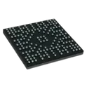
ARM® Cortex®-M33 RT-600 Microcontroller IC 32-Bit Dual-Core 300MHz External Program Memory 176-VFBGA (9x9) The RT600 is a family of dual-core microcontrollers for embedded applications featuring an Arm Cortex-M33 CPU combined with a Cadence Xtensa HiFi4 advanced Audio Digital Signal Processor CPU. The Cortex-M33 includes two hardware coprocessors providing enhanced performance for an array of complex algorithms. The family offers a rich set of peripherals and very low power consumption. The Arm Cortex-M33 is a next generation core based on the ARMv8-M architecture that offers system enhancements, such as ARM TrustZone® security, single-cycle digital signal processing, and a tightly-coupled coprocessor interface, combined with low power consumption, enhanced debug features, and a high level of support block integration. The ARM Cortex-M33 CPU employs a 3-stage instruction pipe and includes an internal prefetch unit that supports speculative branching. A hardware floating-point processor is integrated into the core. On the RT600, the Cortex-M33 is augmented with two hardware coprocessors providing accelerated support for additional DSP algorithms and cryptography. The Cadence Xtensa HiFi 4 Audio DSP engine is a highly optimized audio processor designed especially for efficient execution of audio and voice codecs and pre- and post-processing modules. It supports four 32x32-bit MACs, some support for 72-bit accumulators, limited ability to support eight 32x16-bit MACs, and the ability to issue two 64-bit loads per cycle. There is a floating point unit providing up to four single-precision IEEE floating point MACs per cycle. The RT600 provides up to 4.5 MB of on-chip SRAM (plus an additional 128 KB of tightly-coupled HiFi4 ram) and several high-bandwidth interfaces to access off-chip flash. The FlexSPI flash interface supports two channels and includes an 32 KB cache and an on-the-fly decryption engine. The RT600 is designed to allow the CortexM33 to operate at frequencies of up to 300 MHz and the HiFi4 DSP to operate at frequencies of up to 600 MHz. Key Features Dual-core architecture with Arm Cortex-M33 CPU and Cadence Xtensa HiFi4 DSP Cortex-M33 operating at up to 300 MHz HiFi4 DSP operating at up to 600 MHz Up to 4.5 MB on-chip SRAM 128 KB DSP tightly coupled memory (TCM) FlexSPI interface supporting Quad/Octal SPI Flash with execute-in-place (XIP) High-speed USB 2.0 Host/Device with integrated PHY Digital microphone (DMIC) interface supporting up to 8 channels Multiple I2S, SPI, I²C, UART, SDIO, and I3C interfaces 12-bit ADC with up to 1 MSPS sampling rate Hardware cryptography acceleration (AES, SHA, RSA, ECC) Arm TrustZone® security technology Secure boot and physically unclonable function (PUF) key storage Multiple low-power operating modes for battery-powered applications Up to 147 GPIOs depending on package option 176-pin VFBGA package (9 mm × 9 mm) Typical Applications Voice-controlled smart devices Audio processing and DSP systems Smart speakers and soundbars Industrial HMI and control panels Edge AI and machine learning applications IoT gateways and connected devices Wearable and portable electronics #NXP #iMXRT685 #RT600 #CortexM33 #HiFi4DSP #Microcontroller #EmbeddedSystems #EdgeAI #VoiceRecognition #AudioProcessing #IoT #IndustrialAutomation #SecureMCU #MachineLearning #MCUDesign
3 Uses0 StarsSTM32H743VIT6
ARM® Cortex®-M7 STM32H7 Microcontroller IC 32-Bit 480MHz 2MB (2M x 8) FLASH 100-LQFP (14x14) # STM32H743VIT6 ## General Description The STM32H743VIT6 is a high-performance microcontroller manufactured by STMicroelectronics and based on the Arm Cortex-M7 core. It is designed for advanced embedded applications requiring exceptional processing capability, extensive peripheral integration, high-speed memory access, and real-time control performance. The device combines powerful computational resources, floating-point processing, digital signal processing capabilities, large embedded memory, and a comprehensive set of communication interfaces within a compact package. Its architecture is optimized for industrial automation, motor control, human-machine interfaces, medical devices, robotics, data acquisition systems, audio processing, edge computing, and high-performance IoT applications. ## Key Features ### Processing Architecture * Arm Cortex-M7 processor core * High-performance real-time processing capability * Floating-point unit support * Digital signal processing functionality * Advanced instruction set architecture * Optimized embedded computing performance ### Memory Resources * Embedded Flash memory * High-speed SRAM architecture * Memory protection support * Efficient code and data execution * High-bandwidth memory access capability * Advanced cache architecture ### Communication Interfaces * USART and UART communication interfaces * SPI communication interfaces * I²C communication interfaces * CAN communication support * USB connectivity capability * Ethernet networking support * SDMMC storage interface support * Flexible external communication options ### Analog Features * High-resolution analog-to-digital conversion * Digital-to-analog conversion capability * Precision signal acquisition * Analog monitoring functionality * Sensor interface compatibility ### Timer and Control Features * Advanced control timers * General-purpose timers * PWM signal generation * Encoder interface support * Motor-control functionality * Real-time clock integration * Event-driven control architecture ### Multimedia and Processing Capabilities * Audio processing support * Signal processing applications * Graphics and display interface support * High-speed data acquisition capability * Real-time analytics support * Edge computing functionality ### Power Characteristics * Optimized performance-to-power ratio * Multiple low-power operating modes * Dynamic power management support * Efficient embedded system operation ### Package Characteristics * Surface-mount package construction * Industrial-grade packaging * High-pin-count peripheral integration * Automated assembly compatible * Suitable for complex embedded designs ### Material Construction * Advanced semiconductor technology * RoHS-compliant materials * Lead-free package construction * High-reliability integrated circuit design ### Environmental Characteristics * Suitable for industrial and commercial environments * Long operational service life * Reliable continuous operation * Stable performance across operating conditions * Robust embedded processing platform ### Application Areas * Industrial Automation Systems * Robotics and Motion Control * Motor Drive Applications * Human-Machine Interfaces * Medical Equipment * Audio Processing Systems * Data Acquisition Equipment * Embedded Computing Platforms * Industrial Networking Devices * Edge Computing Solutions * Smart Energy Systems * Advanced IoT Devices * Test and Measurement Equipment * Consumer Electronics ### Compliance * RoHS Compliant * Lead-Free Compatible * Industrial-Grade High-Performance Microcontroller Solution ## Manufacturer STMicroelectronics ## Product Family STM32H7 High-Performance Microcontroller Series #STM32H743VIT6 #STM32H7 #STMicroelectronics #CortexM7 #Microcontroller #EmbeddedSystems #IndustrialAutomation #MotorControl #Robotics #EdgeComputing #IoT #DataAcquisition #EmbeddedDesign #FirmwareDevelopment #ElectronicsEngineering
120 Uses0 StarsSTM32U083CCT6
ARM® Cortex®-M0+ STM32U0 Microcontroller IC 32-Bit 56MHz 256KB (256K x 8) FLASH 48-LQFP (7x7) # STM32U083CCT6 ## General Description The STM32U083CCT6 is an ultra-low-power microcontroller from STMicroelectronics based on the Arm Cortex-M0+ core. It is specifically designed for energy-efficient embedded applications requiring long battery life, advanced peripheral integration, secure operation, and reliable real-time performance. The device combines low-power processing, embedded Flash memory, SRAM, analog peripherals, communication interfaces, and hardware security features within a compact package. Its architecture makes it ideal for smart sensors, industrial monitoring systems, medical devices, wearable electronics, smart metering, home automation products, and Internet of Things applications where power efficiency is a primary design requirement. ## Key Features ### Processing Architecture * Arm Cortex-M0+ processor core * Optimized low-power computing architecture * Efficient real-time processing capability * Interrupt-driven operation support * Embedded system control functionality ### Memory Resources * Embedded Flash memory * Integrated SRAM * Non-volatile data storage support * High-reliability memory architecture * Efficient code execution capability ### Low-Power Features * Ultra-low-power operating modes * Multiple sleep and standby modes * Fast wake-up capability * Battery-powered application optimization * Energy-efficient peripheral operation * Extended product operating life in portable systems ### Security Features * Hardware security mechanisms * Memory protection functionality * Secure firmware execution support * Data integrity protection * Secure embedded application development support ### Communication Interfaces * USART communication interfaces * UART communication support * SPI serial communication interfaces * I²C communication interfaces * Low-power communication capability * Flexible external device connectivity ### Analog Features * Analog-to-digital conversion capability * Precision signal acquisition support * Integrated analog peripherals * Sensor interface compatibility * Low-power analog operation ### Timer and Control Functions * General-purpose timers * PWM signal generation * Real-time clock functionality * Event-driven control capability * Timing and scheduling support ### Package Characteristics * Surface-mount package * Compact footprint design * Automated assembly compatibility * Suitable for space-constrained applications * Industrial-grade packaging ### Material Construction * Advanced low-power semiconductor technology * RoHS-compliant materials * Lead-free package construction * High-reliability integrated circuit design ### Environmental Characteristics * Suitable for industrial and commercial environments * Long operational service life * Stable performance under continuous operation * Robust low-power architecture ### Application Areas * Internet of Things Devices * Smart Sensors * Wearable Electronics * Medical Monitoring Equipment * Home Automation Systems * Smart Metering Applications * Battery-Powered Products * Environmental Monitoring Systems * Industrial Data Acquisition Equipment * Consumer Electronics * Portable Embedded Systems * Wireless Sensor Nodes ### Compliance * RoHS Compliant * Lead-Free Compatible * Industrial-Grade Embedded Microcontroller Solution ## Manufacturer STMicroelectronics ## Product Family STM32U0 Ultra-Low-Power Microcontroller Series #STM32U083CCT6 #STM32U0 #STMicroelectronics #Microcontroller #UltraLowPowerMCU #CortexM0Plus #EmbeddedSystems #IoT #SmartSensors #WearableElectronics #BatteryPoweredDevices #IndustrialElectronics #EmbeddedDesign #FirmwareDevelopment #ElectronicsEngineering
1 Uses0 StarsSTM32H573ZIT6
ARM® Cortex®-M33 STM32H5 Microcontroller IC 32-Bit 250MHz 2MB (2M x 8) FLASH 144-LQFP (20x20) # STM32H573ZIT6 ## General Description The STM32H573ZIT6 is a high-performance microcontroller from STMicroelectronics based on the Arm Cortex-M33 core. It is designed to deliver advanced processing capability, enhanced security, and extensive peripheral integration for industrial, medical, consumer, communications, and embedded control applications. The device combines powerful computational performance with low-power operation, making it suitable for real-time control, edge computing, human-machine interfaces, industrial automation, IoT gateways, motor control systems, and secure connected devices. Integrated security features, high-speed memory architecture, and comprehensive communication interfaces enable the development of robust and scalable embedded solutions. ## Key Features ### Processing Architecture * Arm Cortex-M33 processor core * TrustZone security architecture * Digital signal processing capabilities * Floating-point computation support * Optimized real-time processing performance ### Memory Resources * Embedded Flash memory * Integrated SRAM architecture * Error correction capability for enhanced reliability * High-speed memory access structure ### Security Features * Secure boot functionality * Hardware cryptographic accelerators * Secure firmware update support * Memory protection mechanisms * Tamper detection capabilities * Trusted execution environment * Secure key management support ### Communication Interfaces * USART and UART communication interfaces * SPI serial communication interfaces * I²C communication interfaces * CAN FD connectivity * USB connectivity support * Ethernet interface capability * SDMMC memory card interface * Flexible external communication options ### Analog Features * High-performance analog-to-digital conversion * Digital-to-analog conversion capability * Analog comparators * Precision signal acquisition support ### Timer and Control Functions * Advanced control timers * General-purpose timers * PWM generation capability * Encoder interface support * Motor-control functionality * Real-time clock integration ### Power Characteristics * Low-power operating modes * Dynamic power optimization * Battery-powered application support * Efficient performance-to-power ratio ### Package Characteristics * LQFP package construction * Surface-mount technology compatibility * Industrial-grade mechanical design * Suitable for automated assembly processes ### Application Areas * Industrial Automation Systems * Motor Control Equipment * Human-Machine Interfaces * Smart Energy Systems * Medical Electronics * IoT Gateways * Secure Embedded Devices * Industrial Networking Equipment * Building Automation Systems * Consumer Electronics * Data Acquisition Systems * Edge Computing Applications ### Compliance * RoHS Compliant * Lead-Free Compatible * Industrial and Commercial Application Support ## Manufacturer STMicroelectronics ## Product Family STM32H5 Series High-Performance Microcontrollers #STM32H573ZIT6 #STM32H5 #STMicroelectronics #CortexM33 #Microcontroller #EmbeddedSystems #IndustrialAutomation #SecureMCU #IoT #EdgeComputing #MotorControl #EmbeddedDesign #ElectronicsEngineering #FirmwareDevelopment #IndustrialElectronics
7 Uses0 StarsW25Q128JVSIM
FLASH - NOR Memory IC 128Mb (16M x 8) SPI - Quad I/O, QPI, DTR 133 MHz 8-SOIC 128M-bit Serial Flash Memory with uniform 4KB sectors and Dual/Quad SPI Winbond W25Q128JV is a 128-Mbit (16 MB) serial NOR Flash memory device designed for code and data storage in embedded systems. It supports standard SPI, Dual SPI, Quad SPI (QSPI), and Dual/Quad Peripheral Interface (DPI/QPI) modes, enabling high-speed data transfer rates up to 133 MHz clock operation and up to 532 MB/s equivalent throughput in Quad I/O DTR mode. The device supports Execute-In-Place (XIP), allowing processors and microcontrollers to run code directly from external flash memory without copying it to RAM. Features include 4 KB sector erase, 32 KB and 64 KB block erase, page programming, hardware/software write protection, security registers, JEDEC identification, SFDP support, suspend/resume operations, and low-power standby modes. Suitable for microcontrollers, FPGA configuration storage, IoT devices, industrial controllers, networking equipment, consumer electronics, and embedded systems requiring reliable non-volatile memory. Search Keywords: W25Q128JV, Winbond flash memory, SPI NOR Flash, QSPI Flash, Quad SPI memory, Serial Flash memory, 128Mbit Flash, 16MB Flash memory, Execute In Place XIP, external MCU flash, ESP32 flash memory, FPGA configuration memory, NOR flash storage, W25Q128, Dual SPI Flash, Quad I/O Flash, embedded nonvolatile memory, serial flash IC Hashtags: #W25Q128JV #Winbond #NORFlash #SPIMemory #QSPI #SerialFlash #FlashMemory #EmbeddedSystems #Microcontroller #ESP32 #FPGA #NonVolatileMemory #XIP #IoT #ElectronicsDesign #MemoryIC #FirmwareStorage #QuadSPI #EmbeddedHardware #ElectronicComponents
69 Uses0 Stars