Interface ICs
An interface IC is a type of integrated circuit that is designed to facilitate communication between two devices or systems. These devices are commonly used in electronic systems to enable the transfer of data and control signals between different components or subsystems. Some common use cases for interface ICs include connecting microcontrollers to peripherals such as sensors or displays, linking multiple processors together in a network, and enabling communication between devices using different communication protocols. Flux.ai has the world's largest community-driven public library of interface ICs, with footprints, symbols, datasheets, and simulation models. This library is a valuable resource for engineers and designers who need access to accurate and up-to-date information on these important components. Whether you are working on a new design project or simply looking to learn more about interface ICs, Flux.ai is an excellent resource to help you find the information you need.
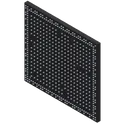
rk3566
BGA-565(15.5x14.4) Microcontrollers, Quad-core ARM Cortex-A55 processor The RK3566 is a high-performance, low-power 64-bit application processor developed by Rockchip for AIoT, industrial control, smart displays, tablets, embedded systems, and single-board computers. It integrates a quad-core ARM Cortex-A55 CPU, Mali-G52 GPU, AI acceleration engine (NPU), advanced multimedia processing, and a rich set of connectivity interfaces, making it suitable for Linux- and Android-based applications requiring efficient performance and multimedia capabilities. Key Features Quad-core 64-bit ARM Cortex-A55 processor operating up to 2.0 GHz. ARM Mali-G52 2EE GPU with support for OpenGL ES 3.2, OpenCL 2.0, and Vulkan 1.1. Integrated NPU delivering up to 1 TOPS AI computing performance. Supports DDR3, DDR3L, DDR4, LPDDR3, LPDDR4, and LPDDR4X memory. Hardware video decoding up to 4K@60fps for H.264, H.265, and VP9 formats. Hardware video encoding up to 1080p@60fps for H.264 and H.265. Built-in 8MP ISP with HDR image processing support. Multiple display interfaces including HDMI 2.0, eDP, MIPI-DSI, LVDS, RGB, and E-Ink. High-speed connectivity with USB 3.0, USB 2.0, PCIe, SATA, Gigabit Ethernet, SDIO, and eMMC 5.1. Rich peripheral support including UART, SPI, I²C, PWM, ADC, I²S, PDM, and GPIO. Optimized for Android, Linux, industrial HMI, smart home, edge computing, and AIoT applications. Manufactured using a 22 nm process for improved power efficiency. #RK3566 #Rockchip #ARMCortexA55 #MaliG52 #AIoT #EmbeddedSystems #SingleBoardComputer #Linux #Android #IndustrialControl #SmartDisplay #EdgeComputing #SoC #Processor #NPU #4KVideo #IoT #Electronics #HardwareDesign #PCBDesign
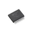
7 Uses0 StarsADN4624BRNZ
5.7 kV RMS/1.5 kV RMS, Quad-Channel LVDS 2.5 Gigabit Isolator (0 Reverse Channels) LVDS Digital Isolator 5700Vrms 4 Channel 2.5Gbps 40kV/µs CMTI 28-BSSOP (0.295", 7.50mm Width) The ADN4624 is a quad-channel, signal isolated, low voltage differential signaling (LVDS) buffer that operates at up to 2.5 Gbps with very low jitter. The device integrates Analog Devices, Inc., iCoupler® technology, enhanced for high speed operation to provide drop-in galvanic isolation of LVDS signal chains. AC coupling and/or level shifting to the LVDS receivers and from the LVDS drivers allows isolation of other high speed signals such as current mode logic (CML). The ADN4624 includes a refresh mechanism to monitor the input and output states and ensure they remain the same in the absence of data transitions (for example, at power-on). For lower power consumption and high speed operation with low jitter, the LVDS and isolator circuits rely on 1.8 V supplies. The ADN4624 is fully specified over a wide industrial temperature range and is available in a 28-lead, wide-body, finer pitch SOIC_W_FP package with 8.3 mm creepage and clearance (for 5.7 kV rms or 8 kVPEAK surge and impulse voltages and reinforced insulation at ac mains voltages) or 6 mm × 6 mm LFCSP package with 1.27 mm creepage and clearance (for basic/functional isolation). FEATURES ► 5.7 kV rms and 1.5 kV rms LVDS isolators ► Complies with TIA/EIA-644-A LVDS signal levels ► Quad-channel configuration ► Any data rate up to 2.5 Gbps switching with low jitter ► 10 Gbps total bandwidth across four channels ► 2.15 ns typical propagation delay ► Typical jitter: 0.82 ps rms random, 40 ps total peak ► Lower power 1.8 V supplies ► ±8 kV IEC 61000-4-2 ESD protection across isolation barrier ► High common-mode transient immunity: 100 kV/μs typical ► Safety and regulatory approvals (28-lead SOIC_W_FP package) ► UL (pending): 5700 V rms for 1 minute per UL 1577 ► CSA Component Acceptance Notice 5A (pending) ► VDE certificate of conformity (pending) ► DIN V VDE V 0884-11 (VDE V 0884-11):2017-01 ► VIORM = 849 VPEAK (working voltage) ► Enable or disable refresh (low speed output correctness check) ► Operating temperature range: −40°C to +125°C ► 28-lead, wide-body, finer pitch SOIC_W_FP package with 8.3 mm creepage and clearance or 6 mm × 6 mm LFCSP package with 1.27 mm creepage and clearance APPLICATIONS ► Isolated video and imaging data ► Analog front-end isolation ► Data plane isolation ► Isolated high speed clock and data links ► Multi-gigabit serialization/deserialization (SERDES) ► Board-to-board optical replacement (for example, short reach fiber) #CommonPartsLibrary #ADN4624BRNZ #DigitalIsolator #LVDS #AnalogDevices #HighSpeedInterface #GalvanicIsolation #LVDSIsolator #DigitalIsolation #IndustrialElectronics #HighSpeedData #SERDES #SignalIntegrity #EmbeddedSystems #ElectronicsDesign #InterfaceICs
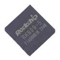
0 Uses0 StarsRK809-5
Rockchip RK809 highly integrated PMIC with audio codec for multi-core system applications, providing five configurable synchronous step-down converters, nine LDO regulators, two switches, battery fuel gauge, configurable power-up/power-down sequencing, integrated RTC with 32.768kHz clock support, I2C interface for voltage and fuel gauge control, dynamic DC/DC output voltage adjustment, soft-start on all channels, 2MHz switching frequency, integrated power switches, headphone driver and Class-D audio driver, QFN68 7.0 x 7.0mm package. Search Keywords: RK809, Rockchip RK809, RK809 PMIC, RK809 power management IC, RK809 codec PMIC, RK809 battery fuel gauge, RK809 audio codec, RK809 DC DC converter, RK809 LDO regulator, RK809 I2C PMIC, RK809 RTC, RK809 QFN68, Rockchip PMIC, RK809 datasheet Hashtags: #RK809 #RockchipRK809 #RockchipPMIC #PMIC #PowerManagementIC #AudioCodecPMIC #BatteryFuelGauge #DCDCConverter #LDORegulator #I2CPMIC #RTC #ClassDAudio #QFN68
1 Uses0 StarsRK809-5
QFN-68-EP(7x7) Power Management - Specialized RoHS The RK809-5 is a highly integrated Power Management Integrated Circuit (PMIC) from Rockchip designed for multi-core processor systems and embedded applications. It provides a complete power management solution by integrating multiple high-efficiency DC-DC buck converters, LDO regulators, power sequencing logic, battery fuel gauging, RTC functionality, and audio codec capabilities into a single device. The RK809-5 is commonly used alongside Rockchip SoCs in single-board computers, tablets, AIoT devices, and industrial embedded systems. Key Features Five high-efficiency synchronous buck converters with fast transient response. Nine low-dropout (LDO) voltage regulators for powering sensitive analog and digital circuits. Integrated battery fuel gauge for battery capacity monitoring. Configurable power-up and power-down sequencing (OTP programmable). Dynamic Voltage Scaling (DVS/DVFS) support via I²C interface. Integrated Real-Time Clock (RTC) with 32.768 kHz crystal oscillator support. Two integrated load switches for peripheral power control. Over-current, over-voltage, and thermal protection features. Built-in audio CODEC with headphone driver and Class-D amplifier support. Designed to minimize external component count and simplify power system design. QFN-68-EP (7 mm × 7 mm) package. #RK8095 #RK809 #Rockchip #PMIC #PowerManagementIC #BatteryManagement #AudioCodec #RTC #DVFS #EmbeddedSystems #SingleBoardComputer #IoT #IndustrialElectronics #PowerSupplyDesign #ElectronicsEngineering
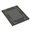
8 Uses0 StarsMT29F256G08AUCABH3-10ITZ:A
SLC NAND Flash Parallel/Serial 3.3V 256G-bit 32G x 8 100-Pin LBGA FLASH - NAND (SLC) Memory IC 256Gbit Parallel 100 MHz 100-LBGA (12x18) The MT29F256G08AUCABH3-10ITZ:A is a high-density 256Gb Single-Level Cell (SLC) NAND Flash memory device from Micron Technology. It provides non-volatile data storage with high reliability, fast read/write performance, and long endurance, making it suitable for industrial, networking, embedded computing, automotive, and data-logging applications. The device supports both asynchronous and synchronous interfaces and complies with the Open NAND Flash Interface (ONFI) standard for enhanced interoperability and performance. It is housed in a compact 100-ball LBGA package (12 mm × 18 mm). • Open NAND Flash Interface (ONFI) 2.2-compliant1 • Single-level cell (SLC) technology • Organization – Page size x8: 8640 bytes (8192 + 448 bytes) – Block size: 128 pages (1024K + 56K bytes) – Plane size: 2 planes x 2048 blocks per plane – Device size: 32Gb: 4096 blocks; 64Gb: 8192 blocks; 128Gb: 16,384 blocks; 256Gb: 32,768 blocks • Synchronous I/O performance – Up to synchronous timing mode 5 – Clock rate: 10ns (DDR) – Read/write throughput per pin: 200 MT/s • Asynchronous I/O performance – Up to asynchronous timing mode 5 – tRC/tWC: 20ns (MIN) – Read/write throughput per pin: 50 MT/s • Array performance – Read page: 35µs (MAX) – Program page: 350µs (TYP) – Erase block: 1.5ms (TYP) • Operating Voltage Range – VCC: 2.7–3.6V – VCCQ: 1.7–1.95V, 2.7–3.6V • Command set: ONFI NAND Flash Protocol • Advanced Command Set – Program cache – Read cache sequential – Read cache random – One-time programmable (OTP) mode – Multi-plane commands – Multi-LUN operations – Read unique ID – Copyback • First block (block address 00h) is valid when shipped from factory. For minimum required ECC, see Error Management (page 114). • RESET (FFh) required as first command after power-on • Operation status byte provides software method for detecting – Operation completion – Pass/fail condition – Write-protect status • Data strobe (DQS) signals provide a hardware method for synchronizing data DQ in the synchronous interface • Copyback operations supported within the plane from which data is read • Quality and reliability – Data retention: JESD47G compliant; see qualification report – Endurance: 60,000 PROGRAM/ERASE cycles • Operating temperature: – Commercial: 0°C to +70°C – Industrial (IT): –40ºC to +85ºC • Package – 52-pad LGA – 48-pin TSOP – 100-ball BGA – 132-ball BGA #Micron #NANDFlash #SLCNAND #FlashMemory #NonVolatileMemory #ONFI #EmbeddedSystems #IndustrialElectronics #DataStorage #MemoryIC #LBGA100 #HighReliability #MT29F256G08AUCABH310ITZA #MicronMemory #ParallelNANDFlash
3 Uses0 StarsATMEGA32U4-AU
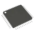
Microchip ATmega32U4 high-performance low-power 8-bit AVR microcontroller with integrated USB 2.0 full-speed device controller, up to 16MHz operation, 32KB Flash memory, 2.5KB SRAM and 1KB EEPROM, 12-channel 10-bit ADC, timers, PWM, SPI, TWI/I2C, USART, JTAG debug interface, watchdog timer, brown-out detection and multiple sleep modes, operating voltage range 2.7V to 5.5V, available in TQFP-44 and QFN-44 packages. Search Keywords: ATmega32U4, Microchip ATmega32U4, Atmel ATmega32U4, AVR USB microcontroller, 8-bit AVR MCU, ATmega32U4 USB, ATmega32U4 TQFP44, ATmega32U4 QFN44, 32KB Flash AVR, Arduino Leonardo MCU, Pro Micro MCU, ATmega32U4 datasheet Hashtags: #ATmega32U4 #MicrochipATmega32U4 #AtmelATmega32U4 #AVRMicrocontroller #8bitMCU #USBMicrocontroller #USBFullSpeed #32KBFlash #ArduinoLeonardoMCU #ProMicroMCU #TQFP44 #QFN44MCU AVR 32K FLASH 16MHZ 44-TQFP Atmel ATMEGA32U4-AU, 8bit AVR Microcontroller, 16MHz, 1 kB, 32 kB Flash, 44-Pin TQFP USB-C Pro Micro ATmega32U4 / Elite-C compatible module
15 Uses0 StarsSTSAFE-A110SO8
STMicroelectronics STSAFE-A110 secure element IC for authentication and secure data management, designed for IoT devices, smart home, smart city, industrial applications, consumer electronics and accessories. Supports authentication to remote or local hosts, secure channel establishment with TLS handshake support, secure boot and firmware upgrade signature verification, host pairing, secure counters, local host envelope wrapping/unwrapping, symmetric data encryption/decryption, on-chip key pair generation, LPWAN security support, ECC cryptography with NIST P-256/P-384, ECDSA, ECDH, SHA-256/SHA-384, 6KB configurable EEPROM, I2C interface, 1.62V to 5.5V supply voltage, -40°C to +105°C operating temperature, available in SO8N and UFDFPN8 packages. Search Keywords: STSAFE-A110, STSAFEA110, STMicroelectronics STSAFE-A110, STSAFE secure element, secure element IC, IoT authentication IC, hardware security IC, secure authentication chip, I2C secure element, ECC secure element, ECDSA ECDH secure chip, TLS authentication IC, secure boot authentication, firmware upgrade security IC, LPWAN security chip, SO8N secure element, UFDFPN8 secure element Hashtags: #STSAFEA110 #STSAFE #STMicroelectronics #SecureElement #AuthenticationIC #IoTSecurity #HardwareSecurity #SecureBoot #FirmwareAuthentication #ECCSecurity #ECDSA #ECDH #TLSHandshake #I2CSecurity #LPWANSecurity #SO8N #UFDFPN8STMicroelectronics Authentication, state-of-the-art security for peripherals and IoT devices
0 Uses0 StarsADS1293CISQ/NOPB
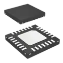
3 Channel AFE 24 Bit 28-WQFN (5x5) ADS1293CISQ/NOPB is a highly integrated, low-power 3-channel ECG Analog Front-End (AFE) from Texas Instruments. It is designed for portable and battery-powered medical devices, fitness monitors, heart-rate monitoring systems, Holter monitors, and other electrocardiogram (ECG) applications. The device integrates signal acquisition, filtering, lead-off detection, right-leg drive generation, and high-resolution analog-to-digital conversion into a single IC, reducing external component count and system cost. Key Features Three high-resolution ECG acquisition channels 24-bit analog-to-digital conversion Simultaneous pace detection support Ultra-low power consumption of approximately 0.3 mW per channel Low input-referred noise of 7 µVpp (40 Hz bandwidth) Programmable sample rates up to 25.6 ksps Differential input voltage range of ±400 mV Integrated EMI-hardened input filters Flexible input routing matrix Built-in Right-Leg Drive (RLD) amplifier AC and DC lead-off detection Integrated Wilson and Goldberger terminal generation Battery voltage monitoring capability Internal oscillator and voltage reference ALARMB pin for interrupt-driven diagnostics and fault reporting Multiple power-down and standby modes for battery-powered systems SPI-compatible digital interface Operating temperature range: –20°C to +85°C 28-pin WQFN package (5 mm × 5 mm) Typical Applications Portable 1-, 3-, 5-, 6-, 7-, 8-, and 12-lead ECG systems Holter monitors Event recorders Telemedicine devices Patient vital-sign monitoring equipment Automated External Defibrillators (AEDs) Sports and fitness heart-rate monitors Wearable medical devices Hashtags #commonpartslibrary #integratedcircuit #TexasInstruments #ADS1293 #AFE #AnalogFrontEnd #ECG #Electrocardiogram #MedicalElectronics #HealthTech #WearableDevices #HeartRateMonitor #PatientMonitoring #BiomedicalEngineering #24BitADC #LowPowerDesign #SPI #SignalConditioning #PortableMedicalDevices #HolterMonitor #Telemedicine #VitalSignsMonitoring #EmbeddedSystems #MixedSignalIC #WQFN28 #BatteryPoweredDevices #MedicalInstrumentation
2 Uses0 StarsPCA9450CHNY
Power Management IC for iMX8M 5V 6A 6 Buck + 5 LDO The PCA9450CHNY is a highly integrated Power Management Integrated Circuit (PMIC) from NXP Semiconductors, specifically designed to power the i.MX 8M family of application processors, particularly the i.MX 8M Plus. It integrates multiple high-efficiency DC-DC buck converters, LDO regulators, power sequencing logic, load switching, voltage monitoring, and system control functions into a single device. The PCA9450C variant features a configurable dual-phase 6 A buck regulator for powering high-current processor cores while supporting Dynamic Voltage Scaling (DVS) for optimized power efficiency. Key Features Six high-efficiency switching regulators (Buck converters) PCA9450C variant supports a configurable 6 A dual-phase buck regulator Three 3 A buck regulators with Dynamic Voltage Scaling (DVS) Remote-sense capability on major buck outputs for IR-drop compensation Five integrated LDO regulators Supports DDR4, LPDDR4, and DDR3L memory configurations 400 mA load switch with active discharge Dual-channel logic level translator Integrated 32.768 kHz crystal oscillator driver Fast-mode Plus (Fm+) 1 MHz I²C interface Programmable power sequencing and voltage control Power ON/OFF and Standby/Run mode control inputs Protection features including UVLO, thermal shutdown, fault monitoring, and soft-start Operating temperature range: −40°C to +105°C 56-pin HVQFN package (7 mm × 7 mm, 0.4 mm pitch) Optimized for i.MX 8M Mini, Nano, and Plus processors, especially the i.MX 8M Plus for the PCA9450C variant. #CommonPartsLibrary #PCA9450CHNY #PCA9450C #NXP #PMIC #PowerManagementIC #PowerSupply #VoltageRegulator #BuckConverter #LDO #DynamicVoltageScaling #DVS #IMX8M #IMX8MPlus #EmbeddedSystems #IndustrialElectronics #PowerManagement #HVQFN56 #Semiconductor #IntegratedCircuit #IC #CommonPartsLibrary #ElectronicsDesign #HardwareDesign #PCBDesign #EmbeddedLinux #IoT #ProcessorPowerManagement #PowerSequencing #SystemPower #NXPSemiconductors
11 Uses0 Stars