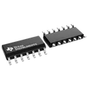
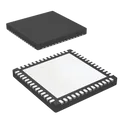
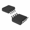
TPSI3100QDVXRQ1
1.5A, 2.5A Gate Driver Magnetic Coupling 5000Vrms 2 Channel 16-SSOP # TPSI3100QDVXRQ1 ## General Description The TPSI3100QDVXRQ1 is an automotive-qualified isolated switch driver manufactured by Texas Instruments and specifically designed for driving solid-state relay architectures based on silicon carbide and gallium nitride power devices. The device integrates an isolated power supply and gate-driver functionality into a compact solution, eliminating the need for external isolated bias supplies in many applications. Its advanced architecture enables reliable control of high-voltage switching systems while providing reinforced isolation, fast switching performance, and enhanced system efficiency. The component is optimized for automotive, industrial automation, energy storage, renewable energy, electric vehicle infrastructure, and high-voltage power conversion applications requiring robust isolation and dependable switching control. ## Key Features ### Isolation Architecture * Integrated isolated switch driver solution * Reinforced isolation technology * High-voltage system compatibility * Enhanced safety and system protection * Reliable signal transfer across isolation barriers * Reduced external component requirements ### Driver Characteristics * Optimized gate-drive functionality * Fast switching performance * Efficient control of solid-state switching devices * Stable drive capability * Low-power control operation * High reliability switching support ### Power Management Features * Integrated isolated power supply * Simplified system architecture * Reduced design complexity * Improved power conversion efficiency * Lower overall component count * Optimized power consumption ### Protection Features * Enhanced electrical isolation * Improved system safety * Reliable operation in high-voltage environments * Robust transient immunity * Stable operation during fault conditions * Protection against electrical stress ### Electrical Characteristics * High-speed switching capability * Low standby power requirements * Reliable signal integrity * Stable operation across operating conditions * Suitable for demanding power electronics applications ### Package Characteristics * Compact surface-mount package * High-density PCB layout support * Automated assembly compatible * Industrial and automotive system integration * Space-efficient implementation ### Material Construction * Advanced semiconductor technology * Automotive-grade manufacturing quality * RoHS-compliant materials * Lead-free package construction * High-reliability integrated circuit architecture ### Environmental Characteristics * Automotive-qualified reliability * Suitable for harsh operating environments * Long operational service life * Stable thermal performance * Reliable continuous-duty operation ### Application Areas * Solid-State Relays * Automotive Electronics * Electric Vehicle Systems * Battery Energy Storage Systems * Renewable Energy Equipment * Industrial Automation Systems * High-Voltage Power Conversion * Motor Drive Systems * Charging Infrastructure * Power Distribution Equipment * Industrial Power Supplies * Advanced Power Electronics ### Compliance * Automotive Qualified * RoHS Compliant * Lead-Free Compatible * Industrial and Automotive Grade Isolated Driver Solution ## Manufacturer Texas Instruments ## Product Family TPSI Isolated Switch Driver Series #TPSI3100QDVXRQ1 #TexasInstruments #IsolatedDriver #SolidStateRelay #GateDriver #AutomotiveElectronics #PowerElectronics #SiliconCarbide #GalliumNitride #IndustrialAutomation #EnergyStorage #ElectricVehicles #PowerConversion #EmbeddedSystems #ElectronicsEngineering... show more0 Uses
0 Stars
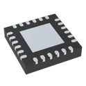
TAA3020IRTER
Audio 16 b, 20 b, 24 b, 32 b 768k I2C, I2S, TDM 20-WQFN (3x3) The TAA3020IRTER is a high-performance 2-channel audio analog-to-digital converter (ADC) from Texas Instruments, designed for professional and embedded audio applications. It supports up to two analog microphone/line inputs or four digital PDM microphone channels with simultaneous sampling. The device delivers excellent audio quality with a 104 dB dynamic range, supports sample rates up to 768 kHz, and integrates advanced audio processing features such as programmable gain, digital filters, automatic gain control (AGC), voice activity detection (VAD), and an integrated PLL. It communicates through an I²C control interface and supports I²S, TDM, and Left-Justified (LJ) digital audio formats, making it ideal for smart speakers, conferencing systems, IP cameras, and other high-performance audio acquisition systems. Key Features High-performance 2-channel audio ADC Supports 2 analog microphone/line inputs or 4 digital PDM microphone inputs 104 dB dynamic range (DR) and –95 dB THD+N Sampling rates from 8 kHz to 768 kHz Programmable microphone gain from 0 dB to 42 dB Digital volume control from –100 dB to +27 dB Integrated programmable HPF, biquad filters, and low-latency filter modes Built-in Automatic Gain Control (AGC) and Voice Activity Detection (VAD) Integrated audio PLL and programmable microphone bias supply Supports I²S, TDM, and Left-Justified (LJ) audio interfaces Configurable for 1.8 V or 3.3 V supply operation Available in a compact 20-pin WQFN (RTE) package Operating temperature range: –40°C to +105°C #AudioADC #TexasInstruments #TAA3020 #HighPerformanceADC #I2S #TDM #PDMMicrophone #AudioProcessing #AGC #VAD #EmbeddedAudio #ProfessionalAudio... show more0 Uses
0 Stars
LMH6574MAX/NOPB
Video Switch IC 1 Channel 14-SOIC The LMH6574MAX/NOPB is a high-speed, 4:1 video multiplexer amplifier manufactured by Texas Instruments. It is designed for routing multiple analog video or high-bandwidth signals into a single output while maintaining excellent signal integrity. With wide bandwidth, low distortion, and fast switching characteristics, it is well-suited for applications such as video switching, RGB routing, medical imaging, and high-speed data acquisition systems. Key Features 4:1 high-speed analog video multiplexer Wide small-signal bandwidth: ~500 MHz (typical) Fast channel switching time: ~8 ns (typical) Low differential gain and phase for video fidelity High slew rate: ~1800 V/µs Low crosstalk and channel-to-channel isolation Single-supply operation: 5 V TTL/CMOS compatible logic inputs Internal 75 Ω back-termination support (video applications) Output disable (high impedance mode) Electrical Characteristics Supply Voltage (Vcc): 4.5 V to 5.5 V Supply Current: ~13 mA (typical) Input Voltage Range: 0 V to Vcc Output Voltage Swing: ~2 Vpp (video typical) Gain: 2 V/V (fixed gain configuration) Input Resistance: High impedance Output Resistance: Low impedance (video drive capable) Dynamic Performance -3 dB Bandwidth: ~500 MHz Slew Rate: ~1800 V/µs Settling Time: ~10 ns Channel Switching Time: ~8 ns Crosstalk: <-60 dB (typical at 10 MHz) Package Information Package Type: SOIC-8 (MAX) Mounting Type: Surface Mount Lead Finish: NiPdAu (RoHS compliant) Operating Temperature Range: -40°C to +85°C Pin Configuration (Summary) 4 Analog Inputs (IN0–IN3) 1 Analog Output (OUT) 2 Digital Select Lines (A0, A1) Enable/Disable Control (EN) Power Supply (Vcc) Ground (GND) Applications Video signal routing and switching (RGB, CVBS) CCTV and broadcast systems Medical imaging equipment Test and measurement instruments High-speed analog multiplexing Data acquisition front-end switching Compliance & Notes RoHS compliant (NOPB = Lead-free package) Designed for 75 Ω video systems Requires proper PCB layout for high-frequency performance (controlled impedance, short traces) #commonpartslibrary #integratedcircuit... show more3 Uses
0 Stars
AFE881H1RRUR
2 Channel AFE 16 Bit 24-UQFN (4x4) The AFE881H1RRUR is a highly integrated analog front-end (AFE) designed for multi-channel data acquisition systems. It combines precision analog signal conditioning with high-speed analog-to-digital conversion, making it suitable for applications such as medical instrumentation, industrial measurement, and test and measurement equipment. The device integrates low-noise amplifiers, programmable gain stages, anti-aliasing filters, and high-resolution ADCs into a compact package, reducing system complexity and board space. Key Features Multi-channel analog front-end integration High-resolution analog-to-digital conversion Low-noise input stage for precision measurements Programmable gain amplifier (PGA) Integrated anti-aliasing filters High sampling rate capability Serial digital interface (SPI-compatible) Low power consumption for portable systems Compact surface-mount package Electrical Characteristics (Typical – refer to datasheet for exact values) Supply Voltage: ~1.8 V to 3.3 V (analog/digital domains) Input Voltage Range: Dependent on configuration Resolution: Up to 16-bit or higher (device dependent) Sampling Rate: Up to several MSPS (depending on mode) Power Consumption: Optimized for performance/power balance Functional Blocks Low-noise input buffer Programmable gain amplifier (PGA) Anti-aliasing filter High-speed ADC core Digital control interface (SPI) Clock management circuitry Package Information Package Type: QFN / VQFN (exact variant per TI RRU package code) Mounting Type: Surface Mount Pin Count: Typically 40+ pins (refer to datasheet for exact count) Applications Medical imaging and instrumentation Industrial data acquisition systems Oscilloscopes and test equipment Communication systems Precision sensor interfaces Advantages High integration reduces external components Improved signal integrity due to low-noise design Flexible configuration via programmable gain Compact footprint for dense PCB layouts Notes Exact electrical parameters, pin configuration, and performance metrics must be verified in the official Texas Instruments datasheet. Proper PCB layout (grounding, shielding, and decoupling) is critical for optimal performance. #commonpartslibrary #integratedcircuit... show more1 Use
0 Stars
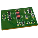
VL53L1X Module
This project is a reference design for a VL53L1X-based sensor circuit. It incorporates the use of a Texas Instruments LP5907MFX-2.8/NOPB to regulate the supply voltage. #referenceDesign #VL53L1X #Module #template #LIDAR #sensor #distance #reusable #module #industrialsensing #stm #sublayout... show more74 Uses
0 Stars
TPS16851VMAR
Hot Swap Controller 1 Channel General Purpose 23-LQFN-CLIP (6x5) The TPS16851VMAR is an automotive-grade integrated electronic fuse device designed to provide advanced power path protection and monitoring for low-voltage DC power distribution systems. The device integrates multiple protection mechanisms including overvoltage protection, undervoltage protection, overcurrent protection, reverse current blocking, and inrush current control within a compact package optimized for space-constrained applications. It is intended for use in automotive, industrial, and embedded electronic systems requiring robust hot-swap capability, fault isolation, and controlled power sequencing. The device incorporates precision current sensing and programmable fault management functions that enable reliable protection of downstream circuitry against abnormal operating conditions. Adjustable protection thresholds and timing parameters allow flexible system-level configuration while maintaining fast fault response and high reliability. Integrated MOSFET control minimizes external component count and simplifies PCB implementation. The TPS16851VMAR supports wide input operating ranges suitable for automotive battery-powered environments and transient-prone supply rails. The device is qualified for harsh operating conditions and includes thermal shutdown and fault reporting features to improve system safety and diagnostics. Engineering Specification Device Type Automotive electronic fuse with integrated protection and power management functionality Manufacturer Texas Instruments Package Type VQFN-HR surface-mount package Mounting Type Surface mount Application Category Automotive power distribution and protection Protection Features Overvoltage protection Undervoltage protection Overcurrent protection Short-circuit protection Reverse current blocking Thermal shutdown Inrush current limiting Control Features Programmable fault thresholds Adjustable current limit Programmable timing and retry behavior Enable and shutdown control Fault indication and monitoring Power Management Features Integrated MOSFET control Hot-swap capability Controlled startup sequencing Load disconnect functionality Interface Characteristics Analog control interface Diagnostic fault reporting Current sense monitoring Operating Environment Automotive-qualified operating conditions High transient immunity Designed for harsh electrical environments PCB Integration Compact footprint Thermally enhanced package Low external component requirement Typical Applications Automotive electronic control units Infotainment systems ADAS power distribution Industrial control systems Embedded power management Protected DC supply rails #commonpartslibrary #integratedcircuit #powermanagement #hotswapcontrollers... show more0 Uses
0 Stars
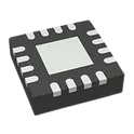
BQ25302RTER
Charger IC Lithium Ion/Polymer 16-WQFN (3x3) The BQ25302RTER is a highly integrated single-cell lithium-ion and lithium-polymer battery charger and power-path management IC developed by Texas Instruments. The device is optimized for compact portable and wearable applications requiring efficient battery charging from USB or low-voltage DC power sources. It integrates a switching charger, power-path management, system voltage regulation, battery FET, and protection features into a compact package suitable for space-constrained designs. The device supports programmable charging current and voltage regulation while maintaining high power conversion efficiency through its switching charger architecture. Integrated power-path management allows the system load to operate simultaneously while charging the battery, improving system reliability and startup behavior when the battery is deeply discharged or absent. The BQ25302RTER includes input current limiting, thermal regulation, battery temperature monitoring support, and multiple safety timers to ensure safe charging operation. The charger automatically manages preconditioning, fast charging, charge termination, and recharge cycles for lithium-based battery chemistries. The device also supports USB-compliant input operation and includes configurable features through an I2C-compatible interface. Its compact WQFN package and high integration level reduce external component count and PCB area, making it suitable for wearable electronics, portable medical devices, IoT products, handheld instruments, wireless accessories, and battery-powered embedded systems. Electrical Characteristics Input operating voltage supports standard USB and low-voltage DC input sources suitable for portable electronics applications. Supports single-cell lithium-ion and lithium-polymer battery charging with programmable charge voltage regulation. Integrated high-efficiency switching charger architecture minimizes power dissipation and improves thermal performance compared to linear chargers. Programmable fast-charge current supports flexible battery capacity scaling and application-specific charging requirements. Integrated power-path management allows simultaneous battery charging and system power delivery. Includes programmable input current limiting to support USB current compliance and adapter protection. Automatic charge cycle management includes precharge, fast charge, termination, and recharge operation. Supports battery temperature qualification using external thermistor monitoring. Integrated thermal regulation dynamically reduces charge current during high-temperature operating conditions. Low quiescent current operation improves standby battery life in portable products. Protection Features Integrated overvoltage protection for input power safety. Battery overcurrent and short-circuit protection enhance system reliability. Thermal shutdown circuitry protects the device during excessive junction temperature conditions. Safety timers monitor charging duration and prevent abnormal charging operation. Input current limiting protects USB ports and weak power adapters from overload conditions. Undervoltage lockout prevents improper operation during insufficient input supply conditions. Interface and Control I2C-compatible serial interface enables configuration and monitoring of charger parameters. Status reporting supports system-level battery and charging management. Programmable charging parameters allow firmware-controlled optimization for different battery chemistries and capacities. Interrupt and status functions support embedded power management architectures. Package Information Supplied in a compact WQFN package optimized for portable and space-constrained PCB layouts. Package design supports efficient thermal dissipation and automated surface-mount assembly processes. RoHS-compliant and suitable for modern lead-free manufacturing requirements. Typical Applications Wearable electronics Wireless earbuds and audio accessories Portable medical devices IoT and embedded battery-powered systems Handheld consumer electronics Portable instrumentation Rechargeable sensor modules Compact USB-powered battery charging systems #CommonPartsLibrary #IntegratedCircuit #PowerManagement #battery charger... show more4 Uses
0 Stars
TPS6593C3A0RWERQ1
Power Management Specialized - PMIC Automotive 2.8-V to 5.5-V PMIC The TPS6593C3A0RWERQ1 is an automotive-grade power management integrated circuit (PMIC) designed by Texas Instruments for advanced processor and system-on-chip power architectures. The device integrates multiple high-efficiency DC/DC buck converters, low-dropout regulators, power sequencing, safety monitoring, and diagnostic functions into a single compact package. It is optimized for use in automotive ADAS, digital cockpit, gateway, radar, vision, and domain controller applications requiring functional safety compliance and high power density. The device supports complex multi-rail power management for high-performance processors and includes configurable startup and shutdown sequencing, voltage monitoring, watchdog functionality, error signaling, and fault protection mechanisms. Integrated communication interfaces enable configuration and monitoring by an external host processor. The PMIC is qualified for automotive applications and supports operation across extended temperature ranges suitable for harsh automotive environments. Key Features Automotive AEC-Q100 qualified power management IC for processor power systems Integrated multi-phase step-down buck converters for high-current rails Integrated low-dropout linear regulators for analog and auxiliary rails Programmable power sequencing and rail management Functional safety support suitable for ASIL-oriented system architectures Integrated watchdog timer and safety monitoring functions Voltage supervision and fault detection for all major rails I2C and SPI communication interface support Power-good outputs and interrupt signaling Thermal shutdown and overtemperature protection Overcurrent and short-circuit protection Undervoltage and overvoltage monitoring Configurable GPIO functionality Low-power standby and sleep mode support Optimized for automotive SoCs and processors High-efficiency switching regulator architecture Compact VQFN package with thermal enhancement Electrical Characteristics Input supply voltage range supports automotive battery-powered systems Multiple programmable buck converter output voltages Integrated LDO outputs for precision analog and digital domains High switching frequency operation for reduced external component size Wide operating junction temperature range suitable for automotive environments Low shutdown current for standby operation High-current capability for processor core supplies Accurate voltage regulation and monitoring Protection and Safety Features Thermal shutdown protection Buck converter cycle-by-cycle current limiting Short-circuit protection on power rails Undervoltage lockout protection Power sequencing fault management Watchdog monitoring for processor supervision Diagnostic interrupt and fault reporting capability Safe-state transition support during fault conditions Package Information Package type: VQFN Package option: RWE Automotive-grade Q1 qualified device RoHS compliant Surface-mount package optimized for thermal performance Typical Applications Automotive domain controllers ADAS processing modules Digital cockpit systems Automotive gateway and networking platforms Radar and vision systems Processor and FPGA power management Industrial high-performance embedded systems #commonpartslibrary #integratedcircuit #powermanagement... show more1 Use
0 Stars
TPS48100QDGXRQ1
High-Side Gate Driver IC Non-Inverting 19-VSSOP The TPS48100QDGXRQ1 is an automotive-grade dual high-side gate driver integrated circuit manufactured by Texas Instruments. It is designed to drive external N-channel power MOSFETs configured as high-side switches, providing the gate-drive voltage and current needed to turn the switches fully on and off with controlled timing. The device targets automotive and other harsh-environment power switching applications where a robust, low quiescent current solution is needed to control loads such as motors, relays, solenoids, lighting, and other inductive or resistive loads powered from a vehicle battery rail. As a member of TI's automotive low-IQ high-side driver portfolio, the device is built to tolerate the wide voltage swings and transient conditions characteristic of automotive electrical systems, including load dump events and cold-crank voltage sags, while maintaining very low standby current draw when the driven loads are not active. This low quiescent current characteristic is particularly valuable in always-on automotive modules, where minimizing parasitic battery drain during vehicle-off states is a key design requirement. The device's two independent driver channels operate synchronously, allowing coordinated control of dual high-side switches from a shared set of control and protection circuitry, which is useful in applications such as dual-channel load switching, H-bridge-adjacent driver stages, or redundant power path control. The non-inverting input structure means that the gate driver outputs follow the logic state of the input control signals directly, simplifying integration with microcontroller-based control logic without requiring additional inverting stages. Internally, the device manages the charge pump or bootstrap circuitry needed to generate a gate voltage above the battery rail, which is necessary to fully enhance an N-channel MOSFET configured in the high-side position. This internal voltage generation simplifies the external bill of materials compared to discrete charge-pump driver implementations. The device is qualified to automotive electronics reliability standards, reflecting the rigorous stress testing and quality requirements expected of components used in vehicle electrical and powertrain-adjacent systems. It is housed in a small-outline surface-mount package suited to space-constrained automotive control module designs, and it is supplied in tape-and-reel or cut-tape packaging formats to support both high-volume automated assembly and lower-volume prototyping needs. Spec Sheet Identification Part Number: TPS48100QDGXRQ1 Device Family: TPS48100-Q1 Manufacturer: Texas Instruments Functional Classification Device Type: Dual high-side gate driver IC Driven Configuration: High-side Channel Type: Synchronous, dual independent drive channels Gate Type Driven: N-channel power MOSFET Input Logic: Non-inverting Electrical Characteristics Supply Voltage Range: Wide automotive-class supply range Quiescent Current: Low-IQ class, optimized for always-on automotive modules Output Drive Current: Symmetric source and sink peak output current Internal Gate Drive Generation: Integrated charge pump/bootstrap-style high-side gate drive generation Protection & Diagnostics Application Context: Suited for protected high-side switching designs typical of the automotive driver family Robustness: Designed to tolerate automotive transient and load-dump conditions Environmental & Qualification Temperature Grade: Extended automotive operating temperature range Automotive Qualification: AEC-Q100 qualified RoHS Compliance: Yes Package Package Type: Small-outline surface-mount package, VSSOP style Mounting: Surface mount technology (SMT) Packaging Format Supply Format: Tape-and-reel, cut-tape, or reel-on-demand packaging options #TPS48100 #TexasInstruments #GateDriver #HighSideDriver #AutomotiveIC #AECQ100 #PowerManagement #MOSFETDriver #LowIQ #VSSOP #SurfaceMount #AutomotiveElectronics #PowerSwitching #SemiconductorIC #EngineeringSpec #ComponentLibrary #CommonPartsLibrary #RoHSCompliant #VehicleElectronics #PCBDesign... show more13 Uses
0 Stars
TPS259540DSGT
All details fully confirmed from Texas Instruments' official datasheet, DigiKey, and multiple verified distributor sources. Here's the complete spec. Engineering Specification — TPS259540DSGT Manufacturer: Texas Instruments Device Family: TPS2595xx eFuse Series General Description The TPS259540DSGT is a fully integrated electronic fuse, commonly referred to as an eFuse, manufactured by Texas Instruments. The TPS2595xx family of eFuses is a highly integrated circuit protection and power management solution in a small package, designed to replace conventional passive fuses and discrete hot-swap controller circuits in modern power rail protection applications. Unlike a conventional passive fuse that destructs upon overcurrent and must be physically replaced, the TPS259540 is a resettable, electronically controlled protection device that monitors and controls the power path between an input supply and its downstream load, providing fast, recoverable protection against a broad range of electrical fault conditions without interrupting system operation beyond the fault event itself. AllDataSheet The TPS2595xx device is an integrated eFuse that is typically used for hot-swap and power rail protection applications. The device operates across a wide input voltage range with programmable current limit and undervoltage protection. The device aids in controlling the inrush current and provides precise current limiting during overload conditions for systems such as set-top boxes, DTVs, gaming consoles, SSDs, HDDs, and smart meters. The device also provides robust protection for multiple faults on the sub-system rail. Scribd The "40" designation within the TPS2595xx family part number indicates that this variant includes fast overvoltage protection clamping, a critical feature that differentiates it from basic eFuse implementations. Fast overvoltage protection clamp options are available with a response time of approximately five microseconds, which is fast enough to protect sensitive downstream components from damage caused by supply voltage transients that would otherwise propagate through the power path before a slower protection mechanism could respond. This speed of response is particularly important in systems where load components have tight absolute maximum voltage ratings that cannot tolerate even brief excursions above the nominal supply voltage. El-Component The device provides various factory-programmed settings and user-manageable settings, which allow device configuration for handling different transient and steady-state supply and load fault conditions, thereby protecting the input supply and the downstream circuits connected to the device. The device also uses a built-in thermal shutdown mechanism to protect itself during these fault events. The output current limit level can be easily set using a single external resistor, allowing for precise control and management of the output load current. Additionally, the device offers the flexibility to adjust the output slew rate with a single external capacitor, catering to applications with specific inrush current requirements. ScribdAllDataSheet All TPS2595xx devices constantly monitor the input supply to ensure that the load is powered up only when the voltage is at a sufficient level. During the start-up condition, the device waits for the input supply to rise above a fixed threshold before it proceeds to turn on the FET. Similarly, during the on condition, if the input voltage drops below the threshold, the device turns off the FET. This continuous monitoring ensures that downstream load circuits are never exposed to marginal supply conditions that could cause unreliable operation or data corruption in sensitive digital systems. Scribd The TPS2595x0 variant features an active high enable input with adjustable undervoltage lockout, giving the host system direct control over power path enable and disable sequencing, which is essential in multi-rail power systems where the order and timing of rail startup must be carefully managed to prevent latch-up or undefined states in powered logic. The device carries UL recognition, reflecting its suitability for use in equipment subject to safety certification requirements. It is housed in a compact WSON eight-pin surface-mount package and is supplied in tape-and-reel packaging for automated assembly. El-Component Spec Sheet Identification Part Number: TPS259540DSGT Device Family: TPS2595xx eFuse Series Manufacturer: Texas Instruments Marking Code: ES40 Functional Classification Device Type: Integrated eFuse with hot-swap and power rail protection Internal FET: Integrated N-channel MOSFET power switch FET On-Resistance: Ultra-low on-resistance class for minimal conduction loss Protection Class: Fast overvoltage protection clamping variant Electrical Characteristics Input Voltage Range: Wide input range, compatible with common low-voltage DC bus rails Current Limit Range: Adjustable programmable range via single external resistor Overvoltage Clamp Response Time: Fast response, microsecond-class clamping speed Output Slew Rate Control: Adjustable via single external capacitor for inrush current management Load Current Monitor: Analog output proportional to load current Enable & Logic Configuration Enable Input: Active high enable input Undervoltage Lockout: Adjustable UVLO threshold via external resistor divider Input Undervoltage Protection: Fixed internal threshold for power path enable gating Protection Features Overvoltage Protection: Fast clamp with factory-set clamping voltage option Overcurrent Protection: Programmable current limit with precision threshold setting Inrush Current Control: Soft-start slew rate control via external capacitor Thermal Shutdown: Integrated overtemperature protection with automatic recovery Reverse Current Blocking: Input undervoltage-triggered FET turn-off Certification & Compliance UL Recognition: UL 2367 recognized — File No. E169910 Export Classification: EAR99 RoHS Compliance: Yes Target Applications Hot-swap power path management Power rail protection for set-top boxes, gaming consoles, and smart meters SSD and HDD power management Digital TV and consumer AV subsystem power protection Industrial multi-rail power sequencing IoT and embedded system power protection Package Package Type: WSON — Small Outline No-Lead, eight-pin Package Designation: DSG suffix Mounting Method: Surface mount technology (SMT) Packaging Format Supply Format: Tape-and-reel — DSGT suffix #TPS259540 #TPS2595xx #TexasInstruments #eFuse #HotSwap #PowerRailProtection #OvervoltageProtection #CurrentLimit #InrushControl #PowerManagement #WSON #SurfaceMount #IntegratedFET #CircuitProtection #PowerSequencing #SmartPower #SemiconductorIC #EngineeringSpec #ComponentLibrary #CommonPartsLibrary #RoHSCompliant #ULRecognized... show more10 Uses
0 Stars
UCC28950TPWRQ1
# UCC28950TPWRQ1 Engineering Specifications **General Description** The UCC28950TPWRQ1 is an automotive-qualified phase-shifted full-bridge controller manufactured by Texas Instruments. It is specifically designed for high-efficiency isolated DC-to-DC power conversion systems requiring advanced control, high power density, and reliable operation in demanding automotive and industrial environments. The device implements phase-shifted pulse-width modulation control with programmable dead-time management to achieve zero-voltage switching across a wide load range. This soft-switching architecture significantly reduces switching losses, improves overall efficiency, minimizes electromagnetic interference, and enables higher switching-frequency operation. The controller integrates comprehensive protection and monitoring functions, including current limiting, overvoltage protection, soft-start control, and fault management. Its flexible architecture supports a wide variety of isolated power-supply topologies used in electric vehicles, onboard charging systems, telecommunications infrastructure, industrial power supplies, and high-performance DC-DC converters. Qualified to automotive reliability standards, the device is suitable for mission-critical applications requiring long-term operational stability and robust power-conversion performance. **Engineering Specifications** **Manufacturer:** Texas Instruments **Manufacturer Part Number:** UCC28950TPWRQ1 **Component Type:** Phase-shifted full-bridge PWM controller **Technology:** Advanced mixed-signal power-management integrated circuit **Control Method:** Phase-shifted pulse-width modulation **Converter Topology:** Full-bridge isolated DC-to-DC converter control **Switching Technique:** Zero-voltage switching support **Efficiency Enhancement:** Reduced switching losses through soft-switching operation **Dead-Time Control:** Programmable adaptive dead-time management **Gate Drive Outputs:** High-current complementary PWM outputs **Current Control:** Cycle-by-cycle current limiting capability **Soft-Start Function:** Programmable startup control **Synchronization Capability:** External synchronization support **Frequency Control:** Programmable switching frequency operation **Feedback Architecture:** Closed-loop voltage regulation support **Fault Management:** Integrated fault detection and shutdown capability **Protection Features:** Overcurrent protection, overvoltage protection, undervoltage lockout, fault shutdown, and soft-start protection **Automotive Qualification:** AEC-Q100 qualified **Reliability Grade:** Automotive-grade performance and reliability **Electromagnetic Compatibility:** Optimized for low-noise power-conversion applications **Power Supply Configuration:** Single-controller power-management operation **Temperature Stability:** Designed for extended automotive operating conditions **Control Flexibility:** Supports a wide range of isolated converter designs **System Integration:** Compatible with high-power MOSFET and IGBT switching stages **Operating Temperature Range:** Automotive temperature range **Package Type:** Thin Shrink Small Outline Package **Package Configuration:** Surface-mount package **Mounting Style:** Surface mount technology **Environmental Compliance:** RoHS compliant and lead-free **Quality Standard:** Automotive production and qualification standards **Typical Applications** Automotive DC-to-DC converters Electric vehicle power systems Battery management systems Onboard charging equipment Telecommunications power supplies Industrial power converters High-power isolated DC-DC modules Server and networking power systems Renewable energy conversion systems Automotive auxiliary power units Motor control power supplies Power-distribution architectures High-efficiency switching power supplies Advanced automotive electronics Mission-critical power-management systems #UCC28950TPWRQ1 #UCC28950 #TexasInstruments #PhaseShiftedFullBridge #PWMController #PowerManagement #DCDCConverter #AutomotiveElectronics #PowerSupplyDesign #ZeroVoltageSwitching #SoftSwitching #ElectricVehicle #IndustrialPower #PowerElectronics #ElectronicComponents #EngineeringSpecifications... show more3 Uses
0 Stars
TPS27S100BRRKT
Power Distribution Switches TPS27S100BRRKT VQFN-16_L4.0-W3.5-P0.50-BL-EP LCSC Part Number: C1849488 TPS27S100 / TPS27S100A / TPS27S100B – single-channel smart high-side power switch with integrated NMOS and charge pump, designed for industrial, automation, telecom, and programmable logic controller (PLC) applications. Supports operating voltages from 3.5 V to 40 V and load currents up to 4 A. Features adjustable current limiting, integrated diagnostics, current monitoring, overload protection, short-circuit protection, thermal shutdown, undervoltage lockout (UVLO), inductive load clamping, and extensive ESD/surge immunity. Available with either digital fault reporting or analog current-sense output for intelligent load management and system protection. Search Keywords: TPS27S100, TPS27S100A, TPS27S100B, Smart High Side Switch, High Side Power Switch, Industrial Load Switch, Protected Load Driver, Current Sense Switch, Industrial Power Distribution, PLC Output Driver, High Side Driver IC, NMOS High Side Switch, Adjustable Current Limit Switch, Short Circuit Protection Switch, Overload Protected Switch, Industrial Automation Power Switch, 24V Load Driver, Telecom Power Switch, Diagnostic Power Switch, Texas Instruments TPS27S100 Hashtags: #TPS27S100 #TPS27S100A #TPS27S100B #TexasInstruments #HighSideSwitch #SmartSwitch #LoadDriver #PowerSwitch #CurrentSense #IndustrialAutomation #PLC #IndustrialControl #TelecomElectronics #PowerDistribution #CircuitProtection #EmbeddedSystems #ElectronicsDesign #PCBDesign #IndustrialElectronics #PowerManagement... show more0 Uses
0 Stars

SN74HC541PWR
SOP65P640X120-20N Texas Instruments 8 7.8mA 2V~6V 7.8mA TSSOP-20 Buffer/Driver/Transceiver ROHS... show more59 Uses
0 Stars
LM66100QDCKRQ1
OR Controller P-Channel 1:1 SC-70-6 Ideal diode that provides reverse polarity protection and power path ORing with a low forward voltage drop. The Texas Instruments LM66100-Q1 operates from 1.5 V to 5.5 V, supports up to 1 A continuous current, features an 11 mΩ (typical) integrated MOSFET, includes reverse current blocking, overvoltage protection up to 6 V, and is offered in a 6-pin SC70 (DCK) package. #IdealDiode #PowerPathProtection #ReverseCurrentBlocking #ReversePolarityProtection #PowerORing #Automotive #TexasInstruments #LM66100Q1 #SC70 #1A #15Vto55V... show more31 Uses
0 Stars
TCAN3404DRBRQ1
Texas Instruments TCAN3404DRBRQ1 automotive 3.3 V CAN FD transceiver with standby, remote wake-up, and ultra-low-power shutdown. Supports classical CAN and CAN FD up to 5 Mbps in certified networks and up to 8 Mbps in simpler networks. DRB 8-pin VSON package, 3 mm × 3 mm, AEC-Q100 qualified.... show more30 Uses
0 Stars
OSD6254-1G-IPM
The OSD6254-1G-IPM is a high-performance System-in-Package (SiP) from Octavo Systems that integrates the Texas Instruments AM6254 processor, 1 GB DDR4 memory, power management circuitry, and essential passive components into a compact 9 × 14 mm BGA package. Featuring a quad-core Arm Cortex-A53 processor with an integrated Cortex-M4F real-time core, it provides a highly integrated solution for industrial automation, IoT gateways, edge AI, HMI, and embedded Linux applications while significantly reducing PCB design complexity and time-to-market. Key Features: Quad-core Arm Cortex-A53 processor (up to 1.4 GHz) Integrated Arm Cortex-M4F real-time co-processor (up to 400 MHz) 1 GB DDR4 memory integrated within the SiP Integrated PMIC and required passive components Rich peripheral interfaces including Ethernet, USB, PCIe, CAN, UART, SPI, I²C, I²S, and SD/MMC Industrial operating temperature range: −40°C to +85°C Compact 9 × 14 mm, 500-ball BGA package Reduces PCB complexity, BOM count, and development time Optimized for embedded Linux, industrial control, HMI, IoT gateway, and edge AI applications #OctavoSystems #OSD6254 #AM6254 #ArmCortexA53 #CortexM4F #SystemInPackage #EmbeddedProcessor #IndustrialAutomation #EdgeAI #IoT #EmbeddedLinux #BGA... show more1 Use
0 Stars
LM74700-Q1
Texas Instruments LM74700-Q1 automotive low-IQ ideal-diode controller for reverse-battery and reverse-current protection. The LM74700QDDFRQ1 drives an external N-channel MOSFET for low-loss power-path control and active ORing, supports 3.2 V to 65 V positive input operation, withstands −65 V reverse voltage, regulates approximately 20 mV forward drop, and provides fast reverse-current blocking with 80 µA typical operating quiescent current. Supplied in the 8-pin DDF SOT-23-THIN package and AEC-Q100 qualified for −40 °C to +125 °C automotive operation.... show more18 Uses
0 Stars
INA826AIDGKR
Texas Instruments 1.10 mm VSSOP-8 Texas Instruments None https://www.snapeda.com/parts/INA826AIDGKR/Texas+Instruments/view-part/?ref=eda IPC-7351B G https://www.snapeda.com/parts/INA826AIDGKR/Texas+Instruments/view-part/?ref=snap INA826AIDGKR... show more37 Uses
0 Stars
TPS25751DREFR
USB Type-C/PD 3.0 controller PMIC in 38-pin WQFN (REF0038A, 4 mm x 6 mm). Texas Instruments TPS25751DREFR provides USB-C port control, USB PD policy/PHY support, I2C host/target interfaces, integrated PP5V/VBUS/PPHV power-path switching, CC/VCONN support, GPIO/ADC configuration pins, and 3.3 V core/I/O supply operation. Key grouped physical pins: PPHV pins 20/21/22, VBUS_IN pins 23/24/25, VBUS pins 32/33, PP5V pins 34/35, exposed pad 39 GND, and exposed pad 40 DRAIN.... show more15 Uses
0 Stars

TPS25751SRSMR
USB Interface IC USB Type-C and USB Power Delivery (PD) controller with integrated power switches 1 595-TPS25751SRSMR https://www.mouser.co.uk/ProductDetail/Texas-Instruments/TPS25751SRSMR?qs=2wMNvWM5ZX4s3a9I%252B6VO9w%3D%3D Texas Instruments TPS25751SRSMR... show more305 Uses
0 Stars
TPS62162DSGR
3.3 V 1 A Synchronous Buck Converter – Step-down DC/DC converter for regulating a 3 V to 17 V input to a fixed 3.3 V output at up to 1 A. The Texas Instruments TPS62162DSGR operates at a typical 2.25 MHz switching frequency and integrates synchronous rectification, power-save mode, power-good output, short-circuit protection, and thermal protection. It is housed in an 8-pin WSON (2 × 2 mm) package and operates from −40°C to +125°C. #TexasInstruments #TPS62162DSGR #BuckConverter #DCDCConverter #VoltageRegulator #PowerManagement #SynchronousBuck #33V #1A #EmbeddedSystems #PCBComponents... show more13 Uses
0 Stars
SN74AHC123AN
Dual Retriggerable Monostable Multivibrator, 2 V to 5.5 V, 16-PDIP Texas Instruments SN74AHC123AN dual retriggerable monostable multivibrator with clear inputs. Generates programmable output pulses from trigger events using external R/C timing components, with Schmitt-trigger circuitry on A, B, and CLR inputs, complementary Q and \overline{Q} outputs, and active PDIP-16 N package ordering. #SN74AHC123AN #DualMonostableMultivibrator #RetriggerableOneShot #SchmittTrigger #2Vto5V5 #ExternalRCTiming #ComplementaryOutputs #PDIP16 #TexasInstruments #74AHC... show more10 Uses
0 Stars
TPS259480AYWPR
Electronic Fuse Regulator High-Side 8A 12-DSBGA (2.43x1.74) eFuse — Texas Instruments TPS259480AYWPR: 3.5 V to 23 V, 8 A eFuse with integrated back-to-back FETs and 12.2 mΩ typical on-resistance. It provides adjustable overvoltage, overcurrent, undervoltage, and output slew-rate control, with reverse-current blocking, load-current monitoring, fast short-circuit protection, and a 12-ball PowerWCSP package. #eFuse #PowerProtection #TexasInstruments #TPS259480AYWPR... show more11 Uses
0 Stars
TUSB320LIRWBR
USB Type-C Configuration Channel (CC) Controller – USB Type-C interface IC that manages port attachment, cable orientation, role detection, and Type-C current detection through the CC1/CC2 pins. The Texas Instruments TUSB320LIRWBR supports DFP (source), UFP (sink), and DRP (dual-role) configurations, with up to 3 A current advertisement/detection. It provides I²C and GPIO control, operates from 2.7 V to 5 V, and is housed in a 12-pin X2QFN (1.6 × 1.6 mm) package for surface-mount assembly. #TexasInstruments #TUSB320LIRWBR #USBTypeC #USBController #CCLogic #TypeC #I2C #GPIO #USBInterface #EmbeddedSystems... show more9 Uses
0 Stars