Designing a PCB from scratch can be time-consuming, especially when ensuring it meets manufacturing constraints. Instead of starting from zero, you can take advantage of Flux’s growing library of templates from leading manufacturers and the community.

The latest addition to this library comes from our collaboration with NextPCB. Their new manufacturing-ready templates provide pre-configured fabrication parameters, reducing guesswork and ensuring a smoother transition to production.

Why Use a Manufacturing-Ready Template?

Starting from a blank PCB layout means manually setting up constraints, verifying design rules, and ensuring compatibility with fabrication processes. NextPCB templates in Flux handle these steps upfront, allowing you to focus on circuit design rather than manufacturability concerns.

Key Benefits:

  • Pre-Defined Manufacturing Constraints – Templates include preset trace widths, via sizes, and clearances aligned with NextPCB’s capabilities.
  • Reduced Design Errors – Built-in constraints minimize potential manufacturing issues.
  • Faster Prototyping – Your designs are ready for production without additional rework.

Available NextPCB Templates

We’ve worked with NextPCB to create a range of templates suitable for different PCB complexities and applications:

  • NextPCB 1-6 Layer BASIC Constraints – Optimized for cost-effective designs that meet NextPCB’s special pricing requirements (PCB dimensions: 30 x 30 to 100 x 100mm).
  • NextPCB 1-4 Layer Standard Constraints – Designed for general-purpose boards to minimize unnecessary costs and complexity.
  • NextPCB 1-4 Layer Complex Constraints – Supports advanced manufacturing features; suitable for more intricate designs.
  • NextPCB 6+ Layer Standard Constraints – Geared towards multi-layer boards where standard design constraints are sufficient.
  • NextPCB 6+ Layer Complex Constraints – Designed for advanced multi-layer designs that require specialized manufacturing capabilities.

Example Project: IoT Sensor Board Using NextPCB Templates

To demonstrate how these templates streamline the design process, we developed a compact IoT-enabled sensor board using one of the NextPCB templates in Flux. This design also takes advantage of NextPCB’s latest Accelerator campaign, which subsidizes users who incorporate the RP2350 microcontroller.

Advantages of Using the Template:

  • Correct Design Rules from the Start – No need for manual input of manufacturing constraints.
  • Optimized Auto-Layout – AI-assisted routing helped achieve a clean, manufacturable layout.
  • Seamless Gerber Export – The design was ready for NextPCB fabrication without additional modifications.

This example highlights how pre-configured templates simplify PCB development, allowing you to iterate and prototype more efficiently.

AI-Powered Design with Flux Copilot & Auto-Layout

Once you’ve selected a template, Flux Copilot and Auto-Layout streamline the design process, allowing you to focus on functionality rather than manual layout work.

  • Component Recommendation – Suggests optimal components and connections based on best practices.
  • AI-Driven Design Suggestions –Copilot provides intelligent recommendations for component selection, based on project requirements and schematics.
  • Optimized Auto-Layout – AI-assisted routing organizes traces efficiently, saving you time and effort.

Exporting and Ordering with NextPCB

Once your design is finalized, NextPCB templates make the transition to manufacturing straightforward. With a single click, you can export your Gerber files, ensuring they align with NextPCB’s fabrication requirements. This eliminates compatibility issues and speeds up the production process.

How to Order PCB & PCBA from NextPCB

NextPCB has recently upgraded its PCB Assembly Quote System, allowing for instant, automated cost estimation. This removes the need for manual review, significantly accelerating the quoting and ordering process.

How to Order PCB & PCBA from NextPCB.

Steps to Order:

  1. Export Gerbers, BOM, and Pick and Place Files from Flux – Before placing your order, export the necessary manufacturing files from Flux. Refer to Flux's documentation for a step-by-step guide on exporting Gerbers, BOM, and Pick and Place files.
  2. Create or Access Your NextPCB Account – Sign up or log in to your NextPCB account.
  3. Navigate to the PCB Quote Page – Proceed to the PCBA quote page.
  4. Upload Your Gerber File – Click on the "Gerber Viewer" button to upload your file.
  5. Specify PCB Quantity – Enter the number of PCBs needed.
  6. Provide Assembly Instructions – Include assembly drawings, pick and place files, and other necessary details.
  7. Upload Your BOM File – Submit your Bill of Materials (BOM) for component sourcing.
  8. Proceed to the Cart – Add your order to the cart and review details.
  9. Review and Confirm Order – Ensure all order details are correct before proceeding.
  10. Select Payment Method & Complete Payment – Choose a payment method and finalize your order.

For more details, visit NextPCB’s official ordering guide.

Get Started with NextPCB Templates in Flux

Leveraging pre-configured templates optimizes your PCB design workflow by integrating manufacturing constraints from the outset. You can iterate faster, reduce potential errors, and ensure manufacturability without additional design rule verification.

Flux already offers a wide range of templates from leading manufacturers and community contributors. If there's a specific template you'd love to see added, let us know! We’re always looking to expand our library with designs that help you build faster and smarter.

Profile avatar of the blog author

Nico Tzovanis

Nico is a professional electronics and PCB design engineer at Flux. Find him on Flux @nico

Go 10x faster from idea to PCB
Work with Flux like an engineering intern—automating the grunt work, learning your standards, explaining its decisions, and checking in for feedback at key moments.
Illustration of sub-layout. Several groups of parts and traces hover above a layout.
Design PCBs with AI
Introducing a new way to work: Give Flux a job and it plans, explains, and executes workflows inside a full browser-based eCAD you can edit anytime.
Screenshot of the Flux app showing a PCB in 3D mode with collaborative cursors, a comment thread pinned on the canvas, and live pricing and availability for a part on the board.

Related Content

Flux for Librarians

Flux for Librarians

Discover how CAD Librarians can leverage Flux’s key capabilities—AI Part Imports, Component Updates, Live Pricing, and JEP30 Export—each tailored to meet the specific demands of maintaining PCB libraries.

Profile avatar of Nico Tzovanis
Nico Tzovanis
|September 13, 2024
Top 20+ Flux Copilot Prompts for Hardware Design

Top 20+ Flux Copilot Prompts for Hardware Design

Explore more than 20 new Flux Copilot prompts for hardware design. Accelerate brainstorming, component selection, validation and design review to streamline your PCB design.

Profile avatar of Lance Cassidy
Lance Cassidy
|August 29, 2024
How to Use Via Stitching in PCB Design

How to Use Via Stitching in PCB Design

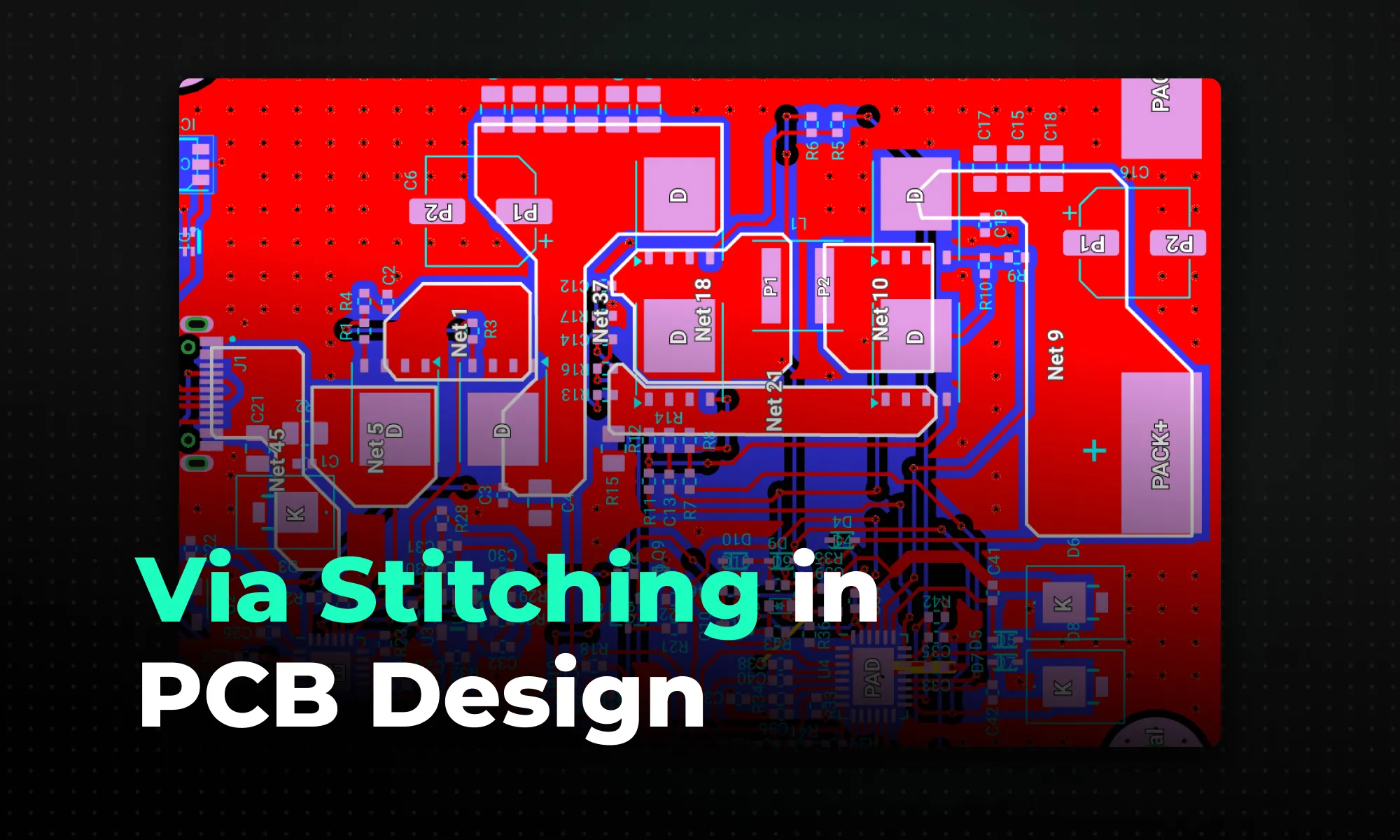
A practical guide to via stitching in PCB design -- what it is, why it improves EMI, signal integrity, and thermal performance, and where to place stitching vias. Includes spacing rules (like lambda/20), design guidelines, common mistakes to avoid, and how Flux can automate stitching via placement.

Profile avatar of Yaneev Hacohen
Yaneev Hacohen
|June 24, 2026
Component Selection in PCB Design: How Engineers Choose the Right Parts

Component Selection in PCB Design: How Engineers Choose the Right Parts

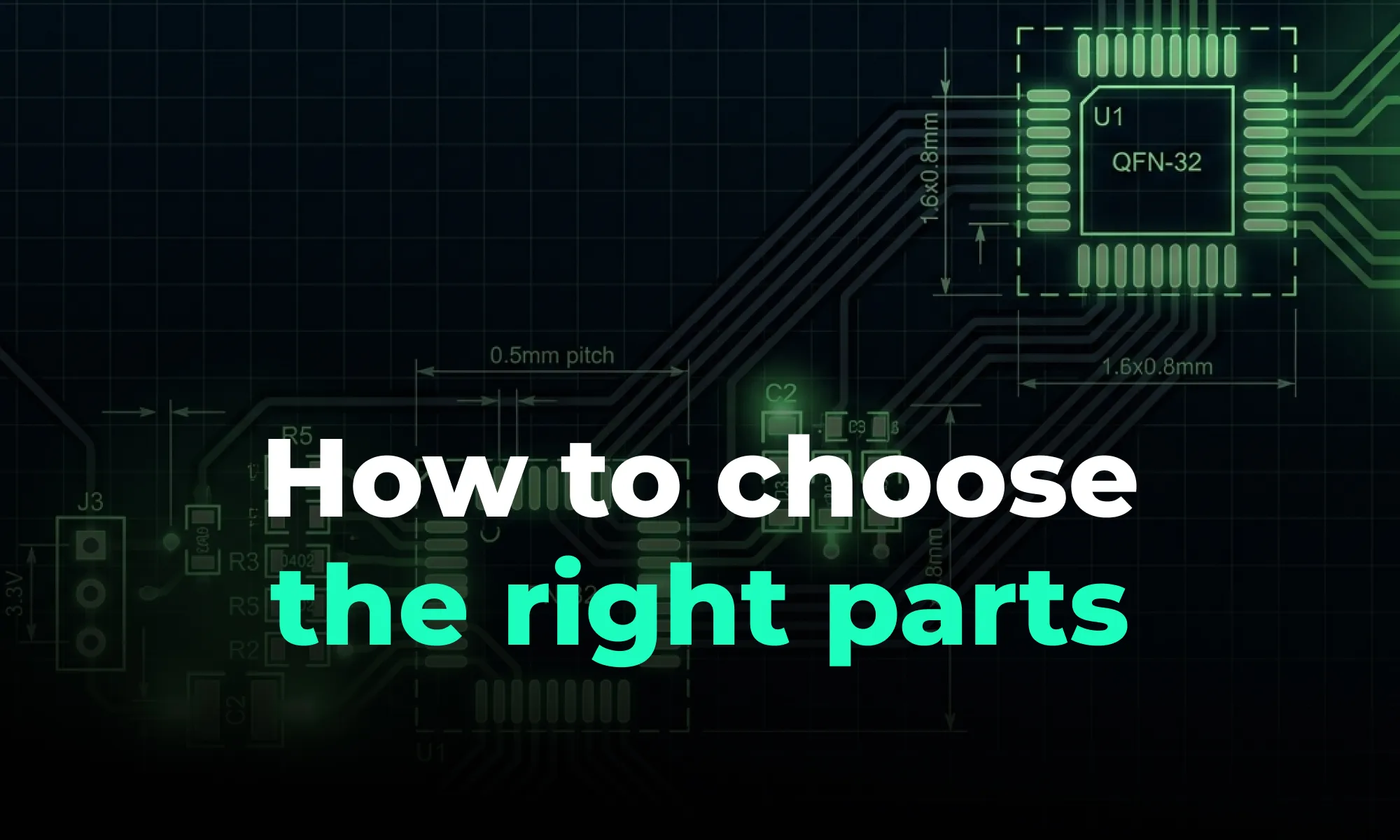
A guide to PCB component selection, covering electrical specs, footprints, thermal performance, sourcing, and best practices for picking parts that ship reliably.

Profile avatar of Yaneev Hacohen
Yaneev Hacohen
|June 15, 2026
PCB Design Reviews: Best Practices for Catching Errors Early

PCB Design Reviews: Best Practices for Catching Errors Early

A guide to PCB design reviews, covering schematic, layout, and DFM checks engineers use to catch errors early and ship more reliable boards.

Profile avatar of Yaneev Hacohen
Yaneev Hacohen
|June 15, 2026
How to Create and Manage PCB Footprint Libraries

How to Create and Manage PCB Footprint Libraries

A guide to creating and managing PCB footprint libraries, covering IPC standards, pad sizing, validation workflows, and best practices for reliable land patterns.

Profile avatar of Yaneev Hacohen
Yaneev Hacohen
|June 15, 2026
PCB Schematic Best Practices for Clean Circuit Design

PCB Schematic Best Practices for Clean Circuit Design

A guide to PCB schematic best practices, covering organization, symbols, labeling, and readability tips for clean, maintainable circuit diagrams.

Profile avatar of Yaneev Hacohen
Yaneev Hacohen
|June 15, 2026
Flexible PCB Design Guide: Materials, Layout, and Applications

Flexible PCB Design Guide: Materials, Layout, and Applications

A guide to flexible PCB design, covering materials, stackups, bend radius, and layout best practices for wearables, medical devices, and other compact electronics.

Profile avatar of Yaneev Hacohen
Yaneev Hacohen
|June 8, 2026